Method for preparing tungsten diselenide semiconductor film on FTO substrate and application of method

A technology of tungsten diselenide and semiconductor, which is applied in the direction of photosensitive equipment, liquid chemical plating, coating, etc., can solve the problem of less film, and achieve the effect of good crystallization, uniform phase and simple preparation process

Active Publication Date: 2017-12-15
GUANGDONG UNIV OF TECH
View PDF7 Cites 5 Cited by
  • Summary
  • Abstract
  • Description
  • Claims
  • Application Information

AI Technical Summary

Problems solved by technology

However, WSe synthesized by solvothermal 2 Most of them are powders (that is, they are first synthesized by solvothermal, th

Method used


Image

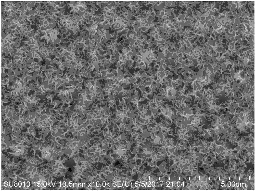
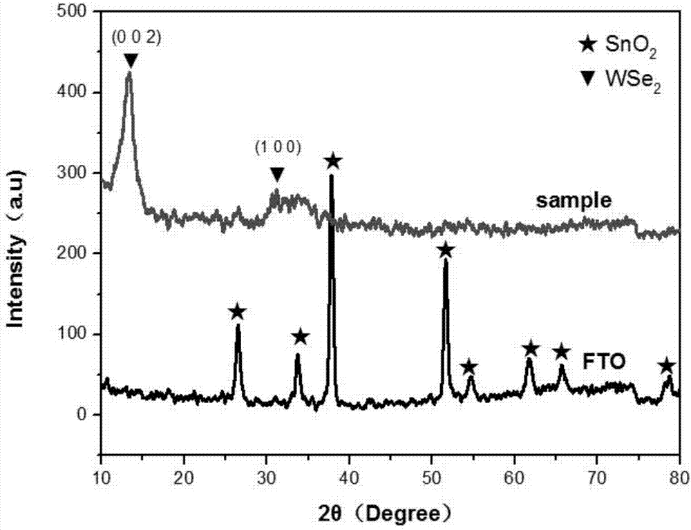
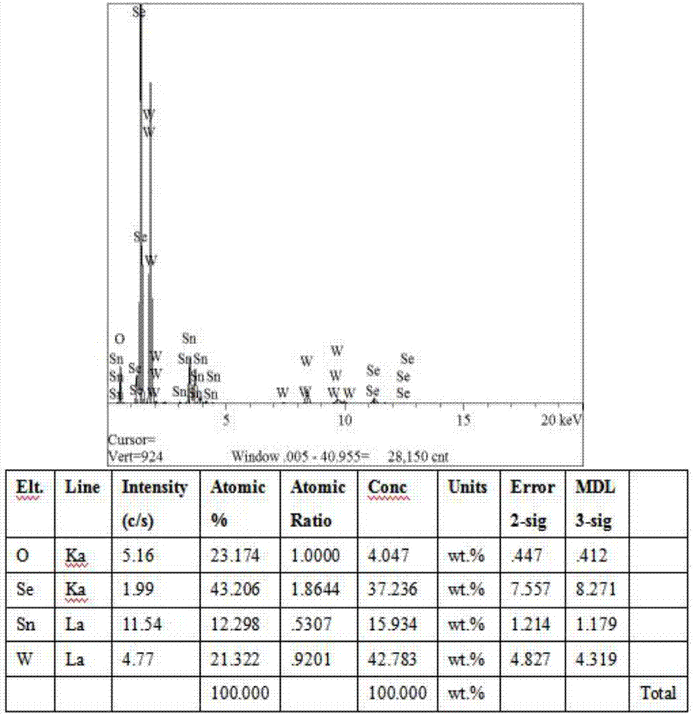
  • Method for preparing tungsten diselenide semiconductor film on FTO substrate and application of method
  • Method for preparing tungsten diselenide semiconductor film on FTO substrate and application of method
  • Method for preparing tungsten diselenide semiconductor film on FTO substrate and application of method

Examples


no. 1 Embodiment

[0043] A method for preparing a tungsten diselenide semiconductor thin film on an FTO substrate, which specifically includes:

[0044] Cleaning steps for FTO conductive glass: place the FTO glass on the cleaning rack, then put it into a beaker, and use acetone, absolute ethanol, and distilled water to clean it ultrasonically for 5 minutes. After cleaning, use clean tweezers to remove the glass piece from the rack. Take it out and dry it with a lint-free cloth;

[0045]After adding 0.20g sodium borohydride into 60ml of DMF, use magnetic stirring until fully dissolved; then, after adding 8.2mmol selenium powder and 4mmol sodium tungstate in sequence, use magnetic stirring for 1 hour until fully dissolved, mix evenly to obtain the reaction precursor liquid;

[0046] Put the cleaned FTO conductive glass into a 100ml clean reactor lining, with the conductive side leaning against the inner wall of the reactor inner substrate; then slowly pour the reaction precursor solution into th...

no. 2 Embodiment

[0049] A method for preparing a tungsten diselenide semiconductor thin film on an FTO substrate, which specifically includes:

[0050] Cleaning steps for FTO conductive glass: place the FTO glass on the cleaning rack, then put it into a beaker, and use acetone, absolute ethanol, and distilled water to clean it ultrasonically for 5 minutes. After cleaning, use clean tweezers to remove the glass piece from the rack. Take it out and dry it with a lint-free cloth;

[0051] After adding 0.20g sodium borohydride into 60ml of DMF, use magnetic stirring until fully dissolved; then, after adding 8.2mmol selenium powder and 4mmol sodium tungstate in sequence, use magnetic stirring for 1 hour until fully dissolved, mix evenly to obtain the reaction precursor liquid;

[0052] Put the cleaned FTO conductive glass into a 100ml clean reactor lining, with the conductive side leaning against the inner wall of the reactor inner substrate; then slowly pour the reaction precursor solution into t...

no. 3 Embodiment

[0055] A method for preparing a tungsten diselenide semiconductor thin film on an FTO substrate, which specifically includes:

[0056] Cleaning steps for FTO conductive glass: place the FTO glass on the cleaning rack, then put it into a beaker, and use acetone, absolute ethanol, and distilled water to clean it ultrasonically for 5 minutes. After cleaning, use clean tweezers to remove the glass piece from the rack. Take it out and dry it with a lint-free cloth;

[0057] After adding 0.22g of sodium borohydride into 60ml of DMF, use magnetic stirring until it is fully dissolved; then, after adding 8.4mmol of selenium powder and 4mmol of sodium tungstate in sequence, use magnetic stirring for 1 hour until it is fully dissolved, and mix evenly to obtain a reaction precursor liquid;

[0058] Put the cleaned FTO conductive glass into a 100ml clean reactor lining, with the conductive side leaning against the inner wall of the reactor inner substrate; then slowly pour the reaction pr...


PUM


Abstract

The invention discloses a method for preparing a tungsten diselenide semiconductor film on an FTO substrate. The method for preparing the tungsten diselenide semiconductor film on the FTO substrate is characterized in that the method comprises the following steps that S1, a reaction precursor solution is prepared, specifically, a solvent, a selenium source, a tungsten source and a reductive agent are evenly mixed to prepare the reaction precursor solution; S2, FTO conductive glass is pretreated, specifically, the FTO conductive glass is subjected to preliminary surface washing treatment; and S3, the tungsten diselenide semiconductor film is prepared, specifically, the treated FTO conductive glass after the step S2 makes contact with the reaction precursor solution prepared in the step S1, and after a sufficient reaction under a high-temperature and high-pressure condition, the tungsten diselenide semiconductor film is prepared on the FTO conductive glass. The method for preparing the tungsten diselenide semiconductor film has the advantages of being simple in preparing technology, low in cost and capable of obtaining the tungsten diselenide semiconductor film which is even in physical phase, good in crystallization and high in purity; and the WSe2 semiconductor film has good prospects in manufacturing of dye-sensitized solar cells and thin-film solar cells.

Description

technical field [0001] The invention relates to the fields of semiconductor thin film preparation technology and new energy development, in particular to a method and application for directly preparing a tungsten diselenide semiconductor thin film on FTO conductive glass based on solvothermal synthesis technology. Background technique [0002] FTO conductive glass is SnO2 transparent conductive glass doped with fluorine F (SnO2: F), referred to as FTO. [0003] For tungsten diselenide (WSe 2 ) thin film, which has a unique energy band structure, good electron transport characteristics, excellent electrochemical catalytic performance, the band gap (1.66eV) is close to the theoretical optimal band gap value of single-junction solar cells, low cost and does not contain Toxic elements, stable performance and other advantages, therefore, it is considered as a good material for the absorbing layer of thin film solar cells. [0004] Currently, the commonly used WSe 2 Thin film p...

Claims


Application Information

Patent Timeline
IPC IPC(8): C23C18/12H01G9/20
Inventor 招瑜温如春庞洲骏陆健婷魏爱香刘俊肖志明李京波
Owner GUANGDONG UNIV OF TECH
Why Eureka
Try Eureka