Multistage unit film transistor memory and preparation method thereof

A thin film transistor and memory technology, which is applied in the field of multi-level unit thin film transistor memory and its preparation, can solve the problems of increased device manufacturing cost and increased device preparation process complexity, and can reduce thermal budget and prevent physical properties and chemical composition from occurring. The effect of changing and reducing the loss of electric charge

Active Publication Date: 2017-12-15
FUDAN UNIV
View PDF8 Cites 14 Cited by
  • Summary
  • Abstract
  • Description
  • Claims
  • Application Information

AI Technical Summary

Problems solved by technology

However, as the size of the device continues to shrink, the complexity of the device manufa

Method used


Image

  • Multistage unit film transistor memory and preparation method thereof
  • Multistage unit film transistor memory and preparation method thereof
  • Multistage unit film transistor memory and preparation method thereof

Examples


preparation example Construction

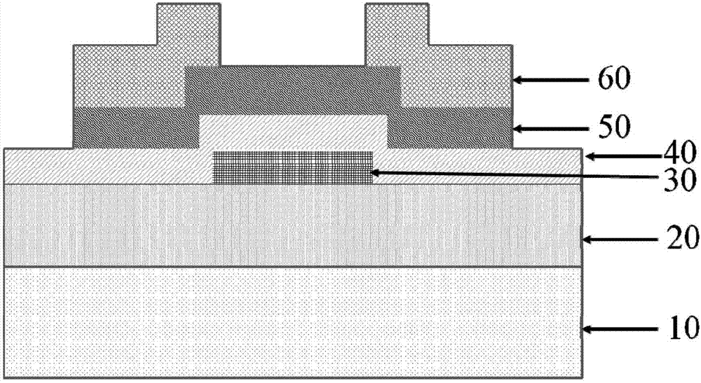
[0040] The present invention also provides a method for preparing the above-mentioned multi-level cell thin film transistor memory, which includes the following steps:

[0041] Step 1, preparing the gate electrode 10;

[0042] Step 2, growing a charge blocking layer 20 on the gate electrode 10 obtained in step 1 by atomic layer deposition, the thickness of the charge blocking layer 20 is 30-60nm, and the deposition temperature is 150-350°C;

[0043]Step 3, growing a charge-trapping layer 30 on the charge-blocking layer 20 obtained in step 2 by atomic deposition or magnetron sputtering deposition, and the thickness of the charge-trapping layer 30 is 10-40 nm;

[0044] Step 4. Spin-coat a layer of positive photoresist on the charge-trapping layer 30 obtained in step 3, then perform photolithography to define the area of ​​the charge-trapping layer 30, and then use a wet etching process to etch the defined area The portion outside the region of the charge trapping layer 30;

[...

Embodiment 1

[0051] In this embodiment, a ZnO thin film is used as the charge trapping layer 30, and the specific preparation process is as follows:

[0052] Step 1, using a P-type monocrystalline silicon wafer with a resistivity of 0.001-0.005Ω·cm as a substrate, and using a standard RCA cleaning process to clean the substrate to form a gate electrode 10;

[0053] Step 2, growing a layer of Al on the gate electrode 10 by ALD method 2 o 3 The film is used as the charge blocking layer 20; the deposition temperature is 150-350°C, preferably 300°C; the film thickness is 30-60nm, preferably 35nm;

[0054] Step 3, growing a layer of ZnO film on the charge blocking layer 20 by ALD method or PVD method as the charge trapping layer 30; the deposition temperature is 150-350°C, preferably 200°C; the film thickness is 10-40nm, preferably 20nm;

[0055] Step 4, spin-coat a layer of positive photoresist on the charge-trapping layer 30, then perform exposure and development to define the region of the...

Embodiment 2

[0063] In this embodiment, an IGZO thin film is used as the charge trapping layer 30, and the specific preparation process is as follows:

[0064] Step 1, using a P-type monocrystalline silicon wafer with a resistivity of 0.001-0.005Ω·cm as a substrate, and using a standard RCA cleaning process to clean the substrate to form a gate electrode 10;

[0065] Step 2, grow a layer of Al on the gate electrode 10 by ALD method 2 o 3 The film is used as the charge blocking layer 20; the deposition temperature is 150-350°C, preferably 300°C; the film thickness is 30-60nm, preferably 35nm;

[0066] Step 3, grow a layer of IGZO film by PVD method on the charge blocking layer 20 as the charge trapping layer 30; the atomic ratio of the IGZO target is In:Ga:Zn:O=1:1:1:4, and the sputtering power is 110W, the working pressure is 0.88Pa, the Ar and O 2 The flow rates are 50sccm and 0sccm respectively; the thickness of the IGZO film is 10-40nm, preferably 20nm;

[0067] Step 4, spin-coat a ...


PUM

PropertyMeasurementUnit
Resistivityaaaaaaaaaa
Thicknessaaaaaaaaaa
Thicknessaaaaaaaaaa

Abstract

The invention discloses a multistage unit film transistor memory and a preparation method thereof; the memory comprises the following units arranged in order from bottom to top: a grid electrode, a charge stop layer, a charge capture layer, a charge tunneling layer, an active area, and a source electrode and a drain electrode; the charge tunneling layer can fully enclose the charge capture layer so as to fully isolate the charge capture layer from the outer side; the charge capture layer is made of a random material from the following group: ZnO, In2O3, Ga2O3, SnO2, InSnO or IGZO. The charge capture layer of the film transistor memory is fully surrounded by the charge tunneling layer, and fully isolated from the outer side, thus preventing the charge capture layer physics property and chemical composition from changing in the technology process, reducing losses of charges stored in the charge capture layer, improving the data maintenance characteristic and device performance stability; the charge capture layer of the memory is made of a metal-oxide semiconductor film, thus realizing multistage unit storage, and improving the storage density.

Description

technical field [0001] The invention relates to the technical field of semiconductor integrated circuit preparation, in particular to a multi-level cell thin film transistor memory and a preparation method thereof. Background technique [0002] Non-volatile memory is an important type of memory, which is widely used in electronic products such as computers, mobile phones, and mobile hard disks, as well as network infrastructure equipment such as servers and network interconnection devices. However, traditional silicon-based nonvolatile memory cannot meet the development needs of next-generation system-on-panel (SOP), future transparent and flexible electronic devices and other fields due to its complex fabrication process and high processing temperature. In recent years, thin-film transistor memory based on a new type of amorphous indium gallium zinc oxide (a-IGZO) semiconductor channel has become a research hotspot in the world. This is because this type of memory has the ...

Claims


Application Information

Patent Timeline
IPC IPC(8): H01L27/11568
CPCH10B43/30G11C16/0466G11C11/5671G11C16/10G11C16/14H01L29/78603H01L29/7869H01L29/66969H01L21/02554H01L21/02565H01L21/02631H01L21/02488H01L29/40117H01L21/02068H01L21/02164H01L21/02175H01L21/02178H01L21/02181H01L21/02189H01L21/02194H01L21/02266H01L21/0228H01L21/0274H01L21/465H01L21/47635H01L29/24H01L29/4234H01L29/45H01L29/513H01L29/517H01L29/7923
Inventor 丁士进钱仕兵刘文军张卫
Owner FUDAN UNIV
Why Eureka
Try Eureka