LED epitaxial growth method

A technology of epitaxial growth and epitaxial structure, applied in electrical components, circuits, semiconductor devices, etc., can solve the problems of increased hole concentration, high optical power, and increased recombination efficiency of holes and electrons in the light-emitting layer

Active Publication Date: 2017-12-15
XIANGNENG HUALEI OPTOELECTRONICS
View PDF6 Cites 7 Cited by
  • Summary
  • Abstract
  • Description
  • Claims
  • Application Information

AI Technical Summary

Problems solved by technology

[0003] However, the driving voltage is limited by the hole mobility of the P layer to a certain extent. The concentration of injected holes increases, the recombination efficiency of h

Method used


Image

  • LED epitaxial growth method
  • LED epitaxial growth method
  • LED epitaxial growth method

Examples


Embodiment 1

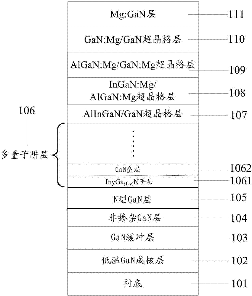
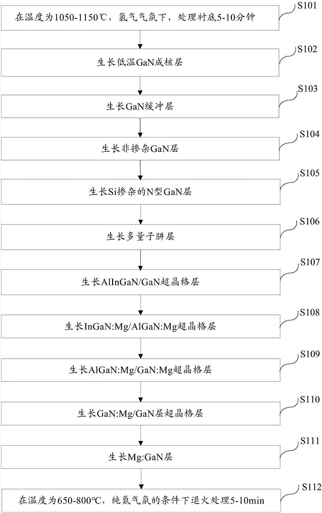
[0065] In order to further reduce the operating voltage of the LED chip and improve the luminous efficiency of the LED chip, this embodiment provides an LED epitaxial growth method, figure 1 A schematic structural diagram of the LED epitaxy prepared by the LED epitaxy growth method in this embodiment is given, please refer to figure 1 , the LED epitaxy, including: a low-temperature GaN nucleation layer 102, a GaN layer 103, a non-doped GaN layer 10 / 4, an N-type GaN layer 105, a multi-quantum well layer 106, an AlInGaN / GaN layer grown on a substrate 101 in sequence Superlattice layer 107 , InGaN:Mg / AlGaN:Mg superlattice layer 108 and AlGaN:Mg / GaN:Mg superlattice layer 109 , GaN:Mg / GaN layer superlattice layer 110 and Mg:GaN layer 111 . Wherein, the multi-quantum well layer 106 includes alternately grown In y Ga (1-y) The alternating period of the N well layer 1061 and the GaN barrier layer 1062 is controlled at 5-15.

[0066] figure 2 The flow chart of the LED epitaxial gr...

Embodiment 2

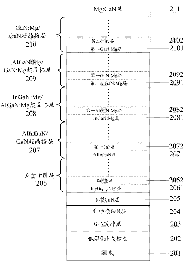
[0094] In order to further reduce the operating voltage of the LED chip and improve the luminous efficiency of the LED chip, this embodiment provides an LED epitaxial growth method, image 3 A schematic structural diagram of the LED epitaxy prepared by the LED epitaxy growth method in this embodiment is given, please refer to image 3 , the LED epitaxy, including: a low-temperature GaN nucleation layer 202, a GaN layer 203, a non-doped GaN layer 204, an N-type GaN layer 205, a multi-quantum well layer 206, and an AlInGaN / GaN supercrystalline layer grown sequentially on a substrate 201 lattice layer 207, InGaN:Mg / AlGaN:Mg superlattice layer 208 and AlGaN:Mg / GaN:Mg superlattice layer 209, GaN:Mg / GaN layer superlattice layer 210 and Mg:GaN layer 211. Wherein, the multi-quantum well layer 206 includes alternately grown In y Ga (1-y) The alternating period of the N well layer 2061 and the GaN barrier layer 2062 is controlled at 5-15.

[0095] Figure 4 The flow chart of the LED...


PUM

PropertyMeasurementUnit
Thicknessaaaaaaaaaa
Thicknessaaaaaaaaaa
Thicknessaaaaaaaaaa

Abstract

The invention provides an LED epitaxial growth method, and the method comprises the steps: sequentially growing an AlInGaN/GaN superlattice layer serving as a final barrier layer and an InGaN:Mg/AlGaN:Mg superlattice layer serving as a hole injection layer, an AlGaN:Mg/GaN:Mg superlattice layer serving as an electron blocking layer and a GaN:Mg/GaN superlattice layer serving as a P-type limiting layer on a multi-quantum well layer. The method can employ a broadband gap comprising an Al material so as to increase the carrier limiting capability, prevents excessive electrons from being leaked to the P layer, employs the characteristic that an In-contained material is not sensitive to dislocation to improve the carrier localization effect, and improves the radiation recombination efficiency. Meanwhile, the method is liable to generate two-dimensional hole air at an interface because of the lattice mismatching of the superlattice layers. The hole lateral expanding efficiency is improved through the two-dimensional hole air, thereby further improving the hole injection level of the quantum well region, reducing the work voltage of an LED and improving the luminous efficiency of the LED.

Description

technical field [0001] The invention belongs to the technical field of LEDs, and in particular relates to an LED epitaxial growth method. Background technique [0002] A light-emitting diode (Light-Emitting Diode, LED) is a semiconductor electronic device that converts electrical energy into light energy. When electric current flows, electrons and holes recombine in it to emit monochromatic light. In order to improve the luminous efficiency of the LED, it is necessary to reduce the driving voltage of the LED, especially the driving voltage under high current, which is also one of the requirements of the market. [0003] However, the driving voltage is limited by the hole mobility of the P layer to a certain extent. As the injected hole concentration increases, the recombination efficiency of holes and electrons in the light-emitting layer increases, and the high optical power increases. Only when the hole mobility of the P layer increases can the driving voltage be reduced....

Claims


Application Information

Patent Timeline
IPC IPC(8): H01L33/06H01L33/14H01L33/32H01L33/00
CPCH01L33/007H01L33/06H01L33/14H01L33/32
Inventor 林传强徐平
Owner XIANGNENG HUALEI OPTOELECTRONICS
Why Eureka
Try Eureka