

Perovskite solar cells based on nano-onion carbon:PC61BM composite electron transport layer
A PC61BM, solar cell technology, applied in circuits, electrical components, photovoltaic power generation, etc., can solve the problems of slow carrier transmission, hysteresis, poor stability, etc., to avoid the decomposition of perovskite structure, increase the number, improve the The effect of fill factor
- Summary
- Abstract
- Description
- Claims
- Application Information
AI Technical Summary
Problems solved by technology
Method used
Image

Examples
Embodiment
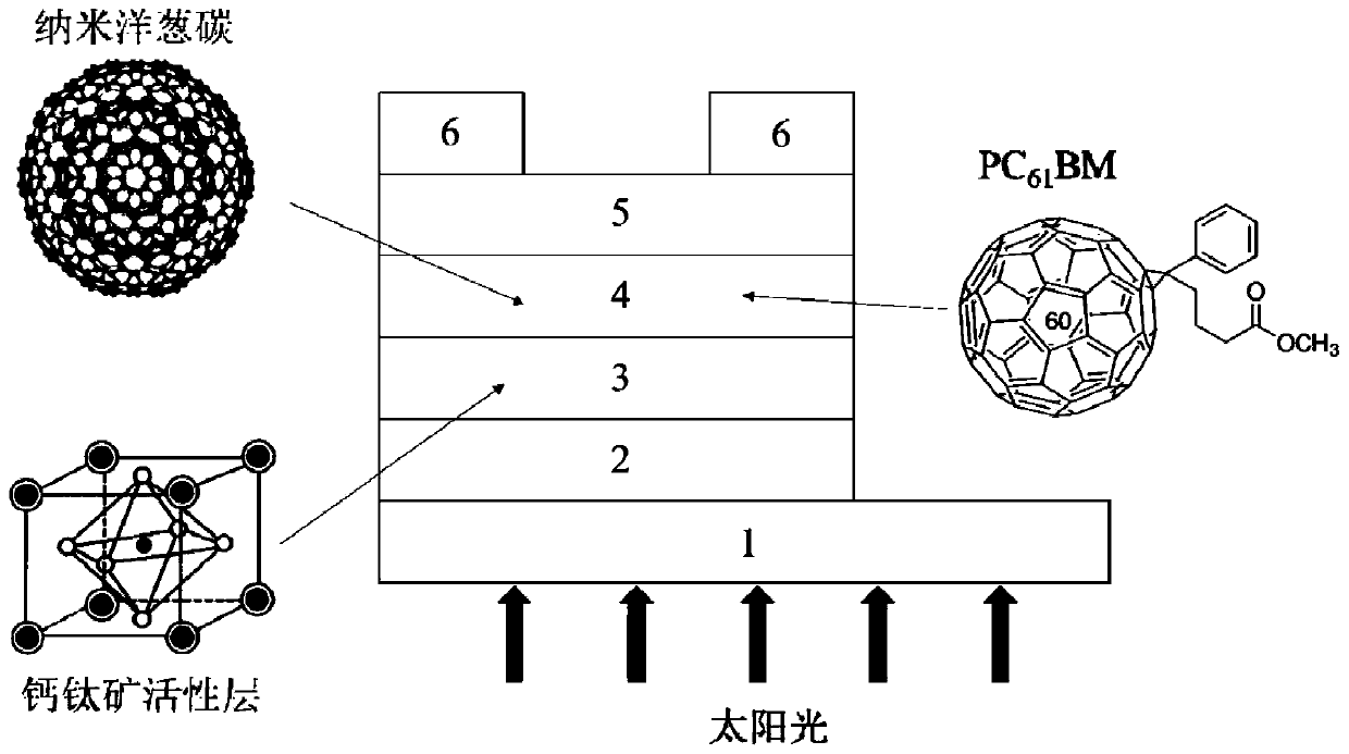
[0030] Such as figure 1 As shown, a nano-onion based carbon: PC 61 A perovskite solar cell with a BM composite electron transport layer, the solar cell adopts a positive structure, including a substrate layer 1, an ITO transparent conductive anode layer 2 (ITO, English name Indium Tin Oxides, that is, indium oxide) arranged in sequence from bottom to top Tin), hole transport layer 3, perovskite photoactive layer 4, composite electron transport layer 5 and metal cathode layer 6;
[0031] in,
[0032] Composite electron transport layer 5 is PC 61 Solid composite layer structure composed of BM material and nano-onion carbon material mixed in proportion;
[0033] Nano-onion carbon materials and PC in composite layer structure 61 The mass percentages of BM materials are:
[0034] Nano-onion carbon 1% to 10%;
[0035] PC 61 BM99%~90%.
[0036] In the above embodiments, the thickness of the ITO transparent conductive anode layer 2 ranges from 20 to 40 nm.
[0037] Preferably...
specific Embodiment
[0045] Control group 1
[0046] Clean the substrate composed of the substrate layer 1 and the ITO transparent conductive anode layer 2 with a surface roughness less than 1nm, and dry it with nitrogen after cleaning; spin-coat the PEDOT:PSS solution on the surface of the ITO transparent conductive anode layer 2 (operating parameters : rotation speed 3000rpm, time 40s) to prepare the hole transport layer 3; and bake the formed film (working parameters: temperature 135°C, time 30min); spin coating on the ITO transparent conductive anode layer 2 to prepare the perovskite light Active layer 4 (thickness 250nm); Spin coating on the surface of perovskite photoactive layer 4 to prepare nano-onion carbon to prepare composite electron transport layer 5 (thickness 20nm; vapor-deposit metal cathode Ag (thickness 100nm, constituting calcium) on metal cathode layer 6 Titanium solar cell devices.
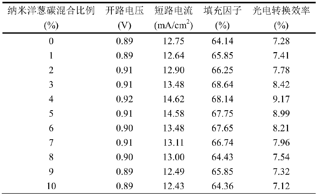
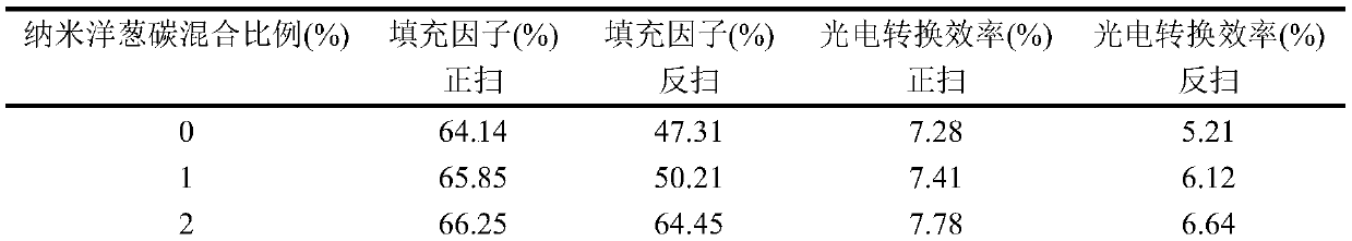
[0047] Under standard test conditions: air quality AM 1.5, light intensity 100mW / cm 2 , the ...
PUM
| Property | Measurement | Unit |
|---|---|---|
| thickness | aaaaa | aaaaa |
| thickness | aaaaa | aaaaa |
| particle diameter | aaaaa | aaaaa |
Abstract
Description
Claims
Application Information