Color-changing organic light emitting diode (OLED) device and fabrication method thereof

A device and intermediate layer technology, applied in the field of color-changing OLED devices, can solve the problems of poor stability, reduction, and short device life, and achieve the effects of variable color, high brightness, and good device stability.

Active Publication Date: 2018-01-09
UNIV OF ELECTRONIC SCI & TECH OF CHINA
View PDF4 Cites 7 Cited by
  • Summary
  • Abstract
  • Description
  • Claims
  • Application Information

AI Technical Summary

Problems solved by technology

[0005] Based on the above technical problems, the present invention provides a color-changing OLED device and its preparation method. The structure of the laminated device is adopted to reduce the voltage required by the series-connected light-emitting layers, and to improve the life of the device while realizing color change, and to optimize the It can achieve good performance, and can solve the shortcomings of the existing color-tunable OLED devices, such as short device life and poor stability, which are caused by different color displays under large external voltage changes.

Method used


Image

  • Color-changing organic light emitting diode (OLED) device and fabrication method thereof
  • Color-changing organic light emitting diode (OLED) device and fabrication method thereof
  • Color-changing organic light emitting diode (OLED) device and fabrication method thereof

Examples


preparation example Construction

[0043] A method for preparing a color-changing OLED device, comprising the following steps:

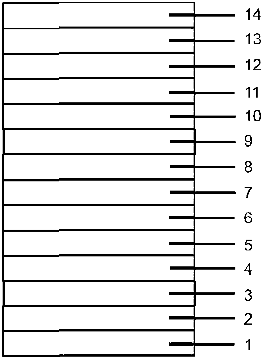
[0044] Step 1, cleaning and drying the ITO glass 1;

[0045] Step 2, move the ITO glass 1 into the vacuum coating chamber, and sequentially vapor-deposit the first hole injection layer 2, the first hole transport layer 3, the first light-emitting layer 4, and the first electron transport layer 5 on the ITO glass 1 , the first electron injection layer 6, the electron type intermediate layer 7, the hole type intermediate layer 8, the second hole injection layer 9, the second hole transport layer 10, the second light emitting layer 11, the second electron transport layer 13, The second electron injection layer and the cathode electrode 14 form an organic electroluminescent device;

[0046] In step 3, the device prepared in step 2 is packaged in a glove box, and the glove box is a nitrogen atmosphere.

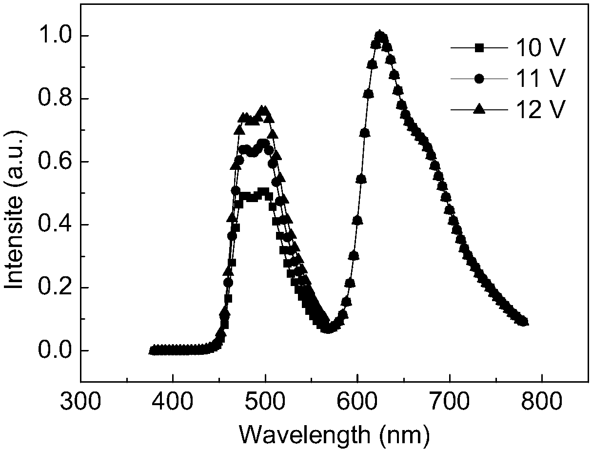
[0047] During the test, the current-voltage-brightness characteristic curve of the d...

Embodiment 1

[0051] Such as figure 1 As shown, the first hole injection layer 2 and the second hole injection layer 9 in the device structure are MoO3 (molybdenum trioxide), and the first hole transport layer 3 and the second hole transport layer 10 are NPB (C44H32N2) , the host material of the first light emitting layer 4 is CBP (C36H24N2), the guest dye is Ir(piq)2(acac)(C35H27N2O2Ir), the first electron transport layer 5 and the second electron transport layer 13 are Bphen(4,7- Biphenyl-1,10-phenanthroline, the first electron injection layer 6 and the second electron injection layer are LiF (lithium fluoride), the electron type intermediate layer 7 is C60 (fullerene), the hole type intermediate layer Layer 8 is CuPc (copper phthalocyanine), the host material of the second light-emitting layer 11 is CBP (C36H24N2), and the guest dye is FIrpic (bis (4,6-difluorophenylpyridine-N, C2) picolinate iridium ), the cathode electrode 14 is aluminum. The whole device structure is described as:

...

Embodiment 2

[0061] Such as figure 1 As shown, the host material of the first light-emitting layer 44 in the device structure is CBP (C36H24N2), and the guest dye is FIrpic (bis (4,6-difluorophenylpyridine-N, C2) picolinate iridium), the first The host material of the second light-emitting layer 1111 is CBP (C36H24N2), and the guest dye is Ir(piq)2(acac)(C35H27N2O2Ir). The entire device structure is described as:

[0062] Glass substrate / ITO / MoO3(3nm) / NPB(30nm) / CBP:10%FIrpic(30nm) / BPhen(40nm) / LiF(1nm) / C60(5nm) / CuPc(5nm) / MoO3(3nm) / NPB(30nm) / CBP:5%Ir(piq)2(acac)(30nm) / BPhen (40nm) / LiF(1nm) / Al(150nm)

[0063] The fabrication process of the device is similar to that of Example 1.

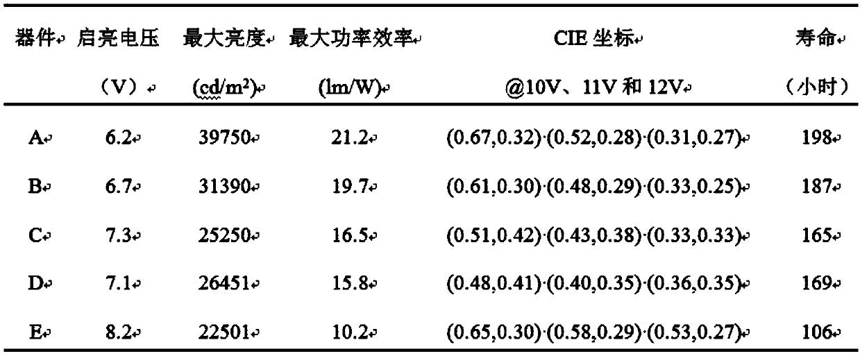
[0064] Device B was produced in Example 2.


PUM

PropertyMeasurementUnit
Resistanceaaaaaaaaaa
Film thicknessaaaaaaaaaa

Abstract

The invention discloses a color-changing organic light emitting diode (OLED) device and a fabrication method thereof, and belongs to the technical field of a light emitting diode device. The inventionaims to provide the color-changing OLED device and the fabrication method thereof. The device comprises ITO glass, a first hole injection layer, a first hole transmission layer, a first light emitting layer, a first electron transmission layer, a first electron injection layer, an electron intermediate layer, a hole intermediate layer, a second hole injection layer, a second hole transmission layer, a second light emitting layer, a second electron transmission layer, a second electron injection layer and a negative electrode. According to the method, the first hole injection layer, the firsthole transmission layer, the first light emitting layer, the first electron transmission layer, the first electron injection layer, the electron intermediate layer, the hole intermediate layer, the second hole injection layer, the second hole transmission layer, the second light emitting layer, the second electron transmission layer, the second electron injection layer and the negative electrode are sequentially evaporated on the ITO glass to form the organic light emitting diode device.

Description

technical field [0001] The invention belongs to the technical field of light-emitting diode devices, and relates to a color-changing OLED device. Background technique [0002] Organic light-emitting diodes (OLEDs) are mainly made of organic light-emitting small molecules and polymers as light-emitting materials, and are prepared by evaporation or spin coating. Currently, OLED lighting products and OLED display panels have been mass-produced. In an OLED display panel, a pixel is usually closely arranged by three-color (red, green, blue) OLED components, and the function of color display is realized by separately adjusting the luminous intensity of the three-color OLED components. Color-tunable organic light-emitting diodes (Color Tunable OLED) can achieve color-tunable functions in a single OLED device, which not only greatly simplifies the manufacturing process, especially the complex mask preparation, thereby reducing the manufacturing cost of OLEDs , and can minimize pixe...

Claims


Application Information

Patent Timeline
IPC IPC(8): H01L51/50H01L51/56
Inventor 于军胜赵聃王子君周殿力
Owner UNIV OF ELECTRONIC SCI & TECH OF CHINA
Why Eureka
Try Eureka