Epitaxial wafer of light-emitting diode and preparation method thereof
A technology for light-emitting diodes and epitaxial wafers, applied in electrical components, circuits, semiconductor devices, etc., can solve the problems of low luminous efficiency of light-emitting diodes, and achieve the effects of promoting plane spreading, increasing doping concentration, and improving uniformity
- Summary
- Abstract
- Description
- Claims
- Application Information
AI Technical Summary
Problems solved by technology
Method used
Image

Examples
Embodiment 1
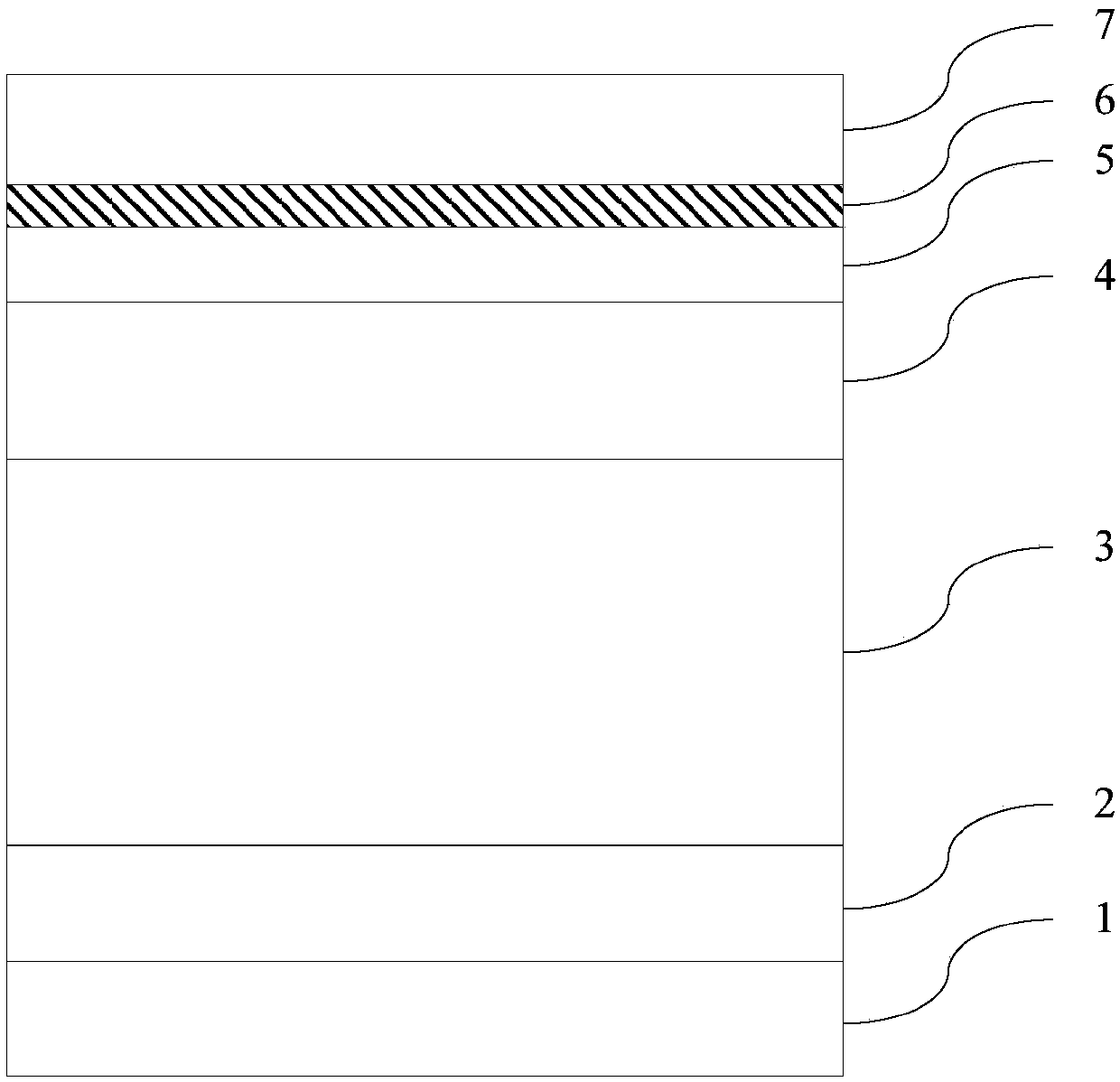
[0029] An embodiment of the present invention provides an epitaxial wafer of a light emitting diode, see figure 1 , the epitaxial wafer includes a substrate 1 and a buffer layer 2, an undoped gallium nitride layer 3, an N-type gallium nitride layer 4, a multi-quantum well layer 5, a hole supply layer 6 and P-type contact layer 7 .
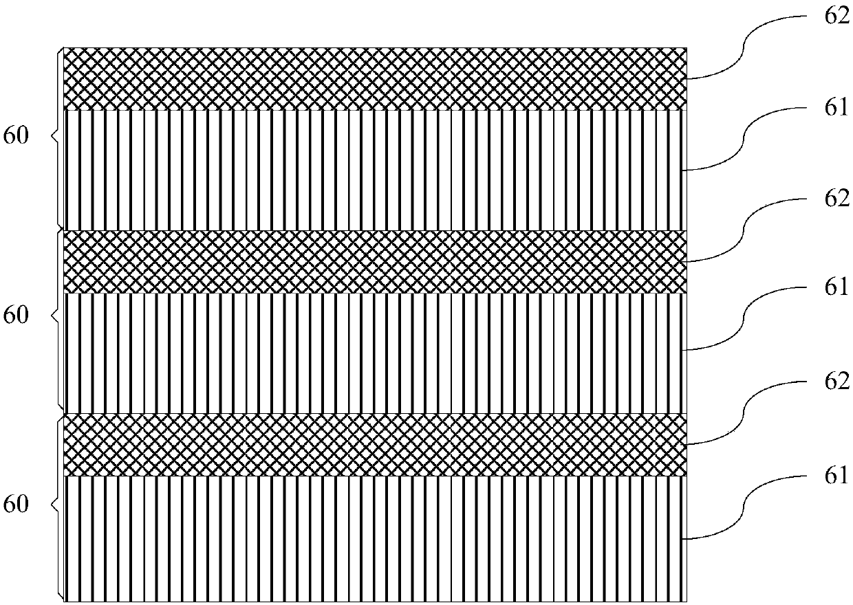
[0030] In this example, see figure 2 , the hole supply layer 6 includes at least one sublayer 60, the sublayer 60 includes a P-type doped InGaN layer 61 and an aluminum nitride layer 62 stacked on the P-type doped InGaN layer 61 ( figure 2 It is only taken as an example that the number of sub-layers is 3, and the present invention is not limited thereto).
[0031] In the implementation of the present invention, the hole-providing layer is changed from a P-type gallium nitride layer to an alternately stacked P-type doped indium gallium nitride layer and an aluminum nitride layer, and the P-type doped indium gallium nitride layer can provide hole...
Embodiment 2
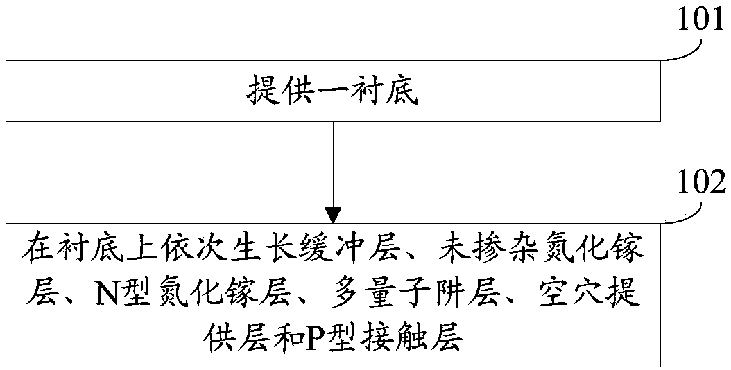
[0047] The embodiment of the present invention provides a method for preparing an epitaxial wafer of a light-emitting diode, which is suitable for preparing the epitaxial wafer provided in Example 1, see image 3 , the preparation method comprises:
[0048] Step 101: Provide a substrate.
[0049] Step 102: sequentially growing a buffer layer, an undoped GaN layer, an N-type GaN layer, a multi-quantum well layer, a hole supply layer and a P-type contact layer on the substrate.
[0050] In this embodiment, the hole supply layer includes at least one sublayer, and the sublayer includes a P-type doped InGaN layer and an AlN layer laminated on the P-type doped InGaN layer.
[0051] In the implementation of the present invention, the hole-providing layer is changed from a P-type gallium nitride layer to an alternately stacked P-type doped indium gallium nitride layer and an aluminum nitride layer, and the P-type doped indium gallium nitride layer can provide holes. The aluminum ni...
Embodiment 3
[0056] An embodiment of the present invention provides a method for manufacturing an epitaxial wafer of a light emitting diode, and the epitaxial wafer provided in this embodiment is a specific implementation of the manufacturing method provided in Embodiment 2. When it is realized, trimethylgallium or trimethylethyl is used as the gallium source, high-purity nitrogen is used as the nitrogen source, trimethylindium is used as the indium source, trimethylaluminum is used as the aluminum source, the N-type dopant is silane, and the P-type dopant is silane. Miscellaneous agent selects dichloromagnesium for use.
[0057] Specifically, see Figure 4 , the preparation method comprises:
[0058] Step 200: Control the temperature to 1000° C. to 1200° C., anneal the sapphire substrate in a hydrogen atmosphere for 8 minutes, and perform nitriding treatment.
[0059] Understandably, step 200 may serve to clean the surface of the sapphire substrate.
[0060] In this embodiment, control...
PUM
| Property | Measurement | Unit |
|---|---|---|
| thickness | aaaaa | aaaaa |
| temperature | aaaaa | aaaaa |
| pressure | aaaaa | aaaaa |
Abstract
Description
Claims
Application Information
 - R&D
- Intellectual Property
- Life Sciences
- Materials
- Tech Scout
- Unparalleled Data Quality
- Higher Quality Content
- 60% Fewer Hallucinations
Browse by: Latest US Patents, China's latest patents, Technical Efficacy Thesaurus, Application Domain, Technology Topic, Popular Technical Reports.
© 2025 PatSnap. All rights reserved.Legal|Privacy policy|Modern Slavery Act Transparency Statement|Sitemap|About US| Contact US: help@patsnap.com