Nano-imprint template as well as making method and application thereof

A technology of nanoimprinting and manufacturing methods, which is applied in the direction of nanotechnology, pattern surface photolithography, semiconductor/solid-state device manufacturing, etc. It can solve problems such as hindering the development of NIL technology, limited process technology, and etching problems, and achieves Improve degumming problem, simple process, easy to operate effect

Inactive Publication Date: 2018-01-30
WUHAN CHINA STAR OPTOELECTRONICS TECH CO LTD
View PDF11 Cites 6 Cited by
  • Summary
  • Abstract
  • Description
  • Claims
  • Application Information

AI Technical Summary

Problems solved by technology

[0004] The wide application of NIL technology in the display field is mainly reflected in the fact that it can achieve better optical performance such as light filtering, anti-reflection, and anti-reflection; however, NIL technology is mostly limited by its manufacturing process, including the production of master molds and soft films. Embossing process and etching process, etc. In the imprinting process, there is often a certain interaction between the material of the mold and the material of the imprinted substrate, resulting in the residue of the material on the substrate or the deformation of the microstructure during the demoulding process, thus also Bring more troubles to subsequent etching
At present, there is no good solution to the problems generated in the imprinting process, which has become one of the bottlenecks hindering the development of NIL technology.

Method used


Image

  • Nano-imprint template as well as making method and application thereof
  • Nano-imprint template as well as making method and application thereof
  • Nano-imprint template as well as making method and application thereof

Examples


Embodiment 1

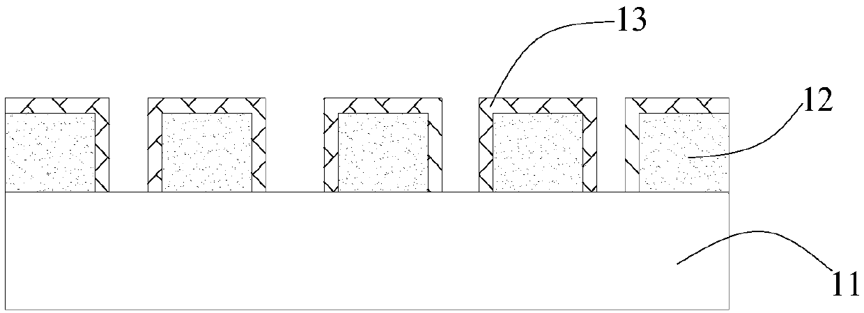
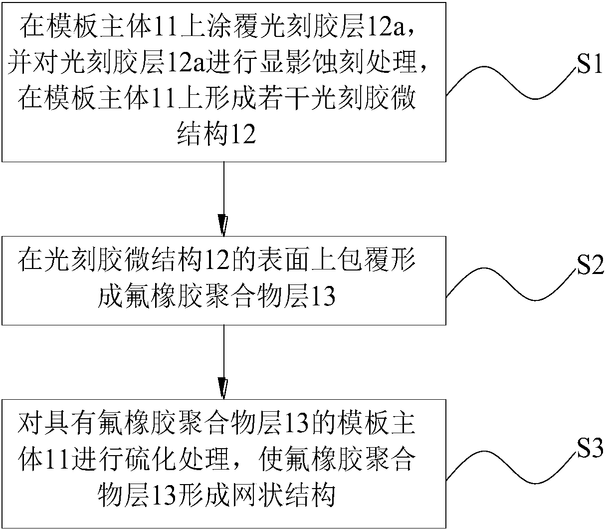
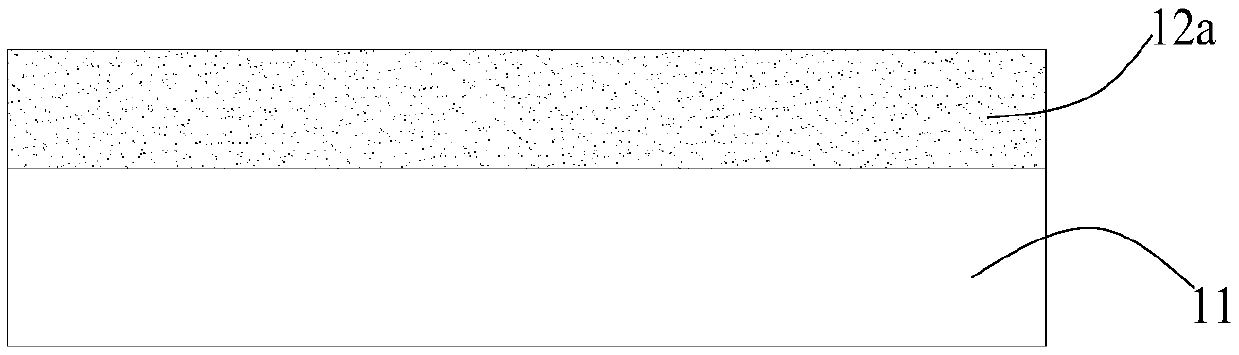
[0036] This embodiment provides a brand new nanoimprint template, refer to figure 1 The nanoimprint template includes a template main body 11 , several photoresist microstructures 12 arranged on the template main body 11 , and a fluororubber polymer layer 13 covering the outer layer of the photoresist microstructures 12 .

[0037] Further, the thickness of the fluororubber polymer layer 12 is 50nm-100nm.

[0038] Furthermore, the material of the fluororubber polymer layer 12 has a structure as shown in formula 1:

[0039]

[0040] In Formula 1, n represents the degree of polymerization, and is not particularly limited here.

[0041] It can be seen from the structural formula of formula 1 that, on the one hand, the silicon oxygen atom group in the main chain of the material of the fluororubber polymer layer 13 can form an interaction with the silicon oxygen atom group in the template main body 11, and the fluororubber polymerizes The role of bonding force can be formed bet...

Embodiment 2

[0059] The purpose of this embodiment is to provide an application of the nano-imprint template as described in the above-mentioned embodiment 1 in the nano-imprint technology, that is, to use the nano-imprint template in the above-mentioned embodiment 1 to fabricate a microstructure substrate.

[0060] The following will refer to Figure 6-Figure 10 The manufacturing method of the microstructure substrate of this embodiment is described in detail. The manufacturing method of the microstructure substrate according to the present embodiment comprises the following steps:

[0061] Step Q1, coating the embossing adhesive layer 22 on the embossing substrate 21; Image 6 shown.

[0062] The imprint substrate 21 is generally selected from flexible substrates such as glass substrates, silicon substrates, and sapphire substrates.

[0063] Step Q2, coating the polytetrafluoroethylene powder layer on the embossed rubber layer 22, and after calcination and cooling treatment, an isolat...


PUM

PropertyMeasurementUnit
thicknessaaaaaaaaaa
thicknessaaaaaaaaaa

Abstract

The invention discloses a nano-imprint template. The nano-imprint template comprises a template main body, a plurality of photoresist microstructures and a fluorine rubber polymer layer, wherein the plurality of photoresist microstructures are arranged on the template main body; the fluorine rubber polymer layer coats outer layers with the photoresist microstructures; a bonding effect exists between the fluorine rubber polymer layer and the template main body, so that the fluorine rubber polymer layer is fixedly connected to the surface of the template main body. The nano-imprint template disclosed by the invention can play a role in protecting the photoresist microstructures in order to prevent the nano-imprint template from being deformed during use, so that the process quality of nano-imprint is enhanced; moreover, the oil resistance and corrosion resistance of the imprinting surface of the nano-imprint template can be improved, the surface has lower surface energy, and the problemof degumming can be effectively improved in an imprinting process. The invention also discloses a making method of the nano-imprint template and application of the nano-imprint template to making of amicro-structure substrate. Through the application method, the microstructure dimension and shape of a formed microstructure substrate can be ensured.

Description

technical field [0001] The invention belongs to the technical field of nano-imprinting, and specifically relates to a nano-imprinting template, a manufacturing method thereof, and a method for using the nano-imprinting template to manufacture a microstructure substrate. Background technique [0002] Due to economic reasons, the semiconductor industry is developing in the direction of continuously reducing the feature size, and the subsequent technological progress has led to an exponential increase in the cost of equipment; There is growing interest in low-cost pattern transfer techniques. By avoiding the use of expensive light sources and projection optics, nanoimprinting offers a substantial cost reduction over traditional photolithography methods. [0003] Due to the omission of the cost of optical lithography masks and the use of optical imaging equipment, NIL technology has the economic advantages of low cost and high output; in addition, NIL technology can be applied ...

Claims


Application Information

Patent Timeline
Patent Type & Authority Applications(China)
IPC IPC(8): G03F7/00B82Y40/00
CPCB82Y40/00G03F7/0002H01L21/0271G03F7/11B29C2059/023
Inventor 杨勇崔宏青
Owner WUHAN CHINA STAR OPTOELECTRONICS TECH CO LTD
Why Eureka
Try Eureka