Dual-trench low-on-resistance and low-gate-charge silicon carbide MOSFET device and preparation method

A low on-resistance, silicon carbide technology, applied in semiconductor/solid-state device manufacturing, semiconductor devices, electrical components, etc., can solve the problem of increased device on-resistance, affecting the downward transmission of electrons, etc., and achieve the reduction of on-resistance , Improve switching characteristics, reduce the effect of device gate charge

Active Publication Date: 2018-02-02
东莞清芯半导体科技有限公司
View PDF6 Cites 11 Cited by
  • Summary
  • Abstract
  • Description
  • Claims
  • Application Information

AI Technical Summary

Problems solved by technology

However, with the introduction of the P+ gate oxide protection region, the depletion region formed in the drift region seriously affects the downward transmission of electrons, making the on-resistance of the device larger

Method used


Image

  • Dual-trench low-on-resistance and low-gate-charge silicon carbide MOSFET device and preparation method
  • Dual-trench low-on-resistance and low-gate-charge silicon carbide MOSFET device and preparation method
  • Dual-trench low-on-resistance and low-gate-charge silicon carbide MOSFET device and preparation method

Examples


Embodiment Construction

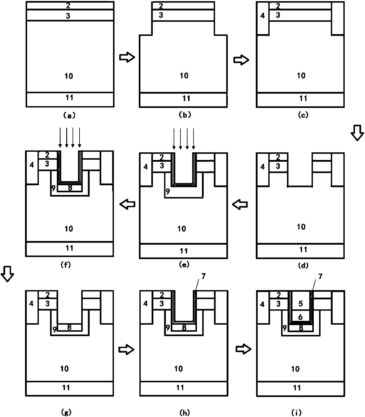
[0042] The implementation of the present invention will be described in detail below in conjunction with the drawings and examples.

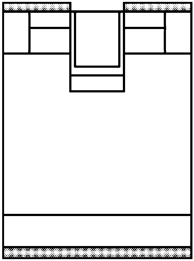
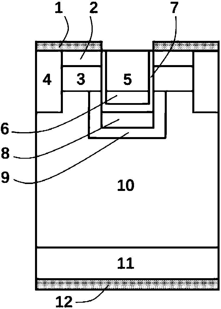
[0043] Traditional SiC power MOSFET structures such as figure 1 shown, including:

[0044] a polysilicon gate 5 of the first conductivity type;

[0045] The trench gate dielectric 7 wrapping the first conductive type polysilicon gate 5;

[0046] A source electrode 1 with a symmetrical structure arranged on both sides of the trench gate dielectric 7;

[0047] The first conductive type source contact region 2, the second conductive type base region 3 and the heavily doped second conductive type trench region 4 arranged at the bottom of the source electrode 1; the first conductive type source contact region 2 and the lower part of the source electrode 1 , the upper part of the second conductive type base region 3 and the side surface of the heavily doped second conductive type trench region 4 are in contact with the lower part of the source electr...


PUM

PropertyMeasurementUnit
thicknessaaaaaaaaaa
thicknessaaaaaaaaaa
thicknessaaaaaaaaaa

Abstract

Disclosed are a dual-trench low-on-resistance and low-gate-charge silicon carbide MOSFET device and a preparation method. The device comprises a source, a first conductive type source region contact part, a second conductive type base region, a heavily-doped second conductive type trench region, a first conductive type polysilicon gate, a second conductive type polysilicon gate, groove gate dielectric, a second conductive type gate oxide protection region, a first conductive type packaging region, a first conductive type drift region, a first conductive type substrate and a drain. By virtue ofa space charge region formed by the first conductive type polysilicon gate and the second conductive type polysilicon gate, coupling between the gate and the drain is lowered, thereby lowering gate charge of the device; by virtue of the first conductive type packaging region, the space charge region formed by the second conductive type gate oxide protection region in the drift region can be reduced; in addition, effective current transmission can be realized, so that the on resistance of the device can be lowered; and by virtue of the heavily-doped second conductive type trench region, the gate oxide electric field can be shielded effectively, and the gate oxide can be protected.

Description

technical field [0001] The invention relates to the field of silicon carbide power devices for microelectronics and power electronics, in particular to a silicon carbide MOSFET device with double grooves, low on-resistance and small gate charge and a preparation method. Background technique [0002] Wide bandgap semiconductor silicon carbide, because of its large bandgap, high thermal conductivity, high breakdown field strength, high electron saturation velocity and strong radiation resistance, makes silicon carbide power semiconductor devices applicable radiation working environment. In the field of power electronics, power MOSFETs are widely used due to their advantages such as simple driving circuits and short switching times. [0003] In the power MOSFET device, the lateral power MOSFET has a large on-resistance due to the parasitic JFET area, while in the vertical structure power trench gate MOSFET device, its structure design eliminates the JFET area, which greatly re...

Claims


Application Information

Patent Timeline
Patent Type & Authority Applications(China)
IPC IPC(8): H01L29/78H01L29/423H01L21/04H01L29/06H01L21/336
CPCH01L21/049H01L29/0684H01L29/4236H01L29/66068H01L29/7827
Inventor 张安平田凯祁金伟杨明超陈家玉王旭辉曾翔君李留成
Owner 东莞清芯半导体科技有限公司
Why Eureka
Try Eureka