

Oxide thin film transistor and its preparation method, array substrate and display device
An oxide thin film and transistor technology, applied in transistors, semiconductor/solid-state device manufacturing, semiconductor devices, etc., can solve the problems of inconsistent three-layer metal etching rate, easy formation of eaves, chamfering, damage, etc., to reduce the patterning process. times, reducing the number of metal layers, and improving electrical performance
- Summary
- Abstract
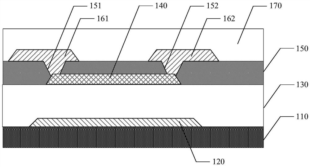
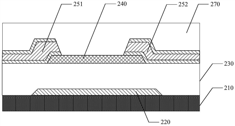
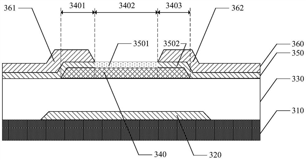
- Description
- Claims
- Application Information
AI Technical Summary
Problems solved by technology
Method used
Image

Examples
Embodiment Construction
[0034] In order to make the above objects, features and advantages of the present invention more clearly understood, the present invention will be described in further detail below with reference to the accompanying drawings and specific embodiments.
[0035] In the description of the present invention, unless otherwise stated, "plurality" means two or more; the terms "upper", "lower", "left", "right", "inner", "outer" The orientation or positional relationship indicated by etc. is based on the orientation or positional relationship shown in the accompanying drawings, which is only for the convenience of describing the present invention and simplifying the description, rather than indicating or implying that the referred machine or element must have a specific orientation, a specific orientation, and a specific orientation. The orientation configuration and operation are therefore not to be construed as limitations of the present invention.
[0036] In the description of the p...
PUM
 Abstract
Description
Claims
Application Information