Composite-window-layer cadmium-telluride film solar cell and preparing method thereof
A solar cell and window layer technology, applied in circuits, photovoltaic power generation, electrical components, etc., can solve problems such as the reduction of photoelectric conversion efficiency, the loss of electrons or carriers between the cadmium sulfide window layer and the substrate, and the impact on current density.
- Summary
- Abstract
- Description
- Claims
- Application Information
AI Technical Summary
Problems solved by technology
Method used
Image
Examples
preparation example Construction
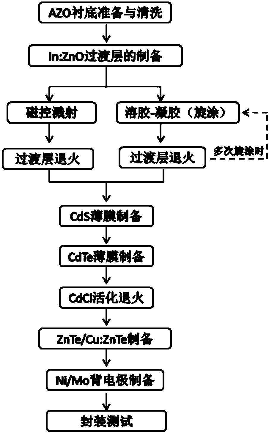
[0030] Its preparation method comprises the following steps:
[0031] (1) AZO glass doped with aluminum zinc oxide is used as the substrate layer, and a layer of indium-doped zinc oxide is deposited as a window transition layer on the substrate layer, and then annealed, and the deposition method is magnetron sputtering or sol-gel glue method; (2) adopt space sublimation method to deposit cadmium sulfide window layer on described window transition layer; (3) adopt space sublimation method to deposit cadmium telluride light absorbing layer on described cadmium sulfide window layer, use CdCl 2 Carry out activation treatment, then annealing treatment; (4) adopt magnetron sputtering method to deposit back contact layer on described cadmium telluride light absorbing layer; (5) adopt magnetron sputtering method to deposit back contact layer on described back contact layer electrode layer.
Embodiment 1
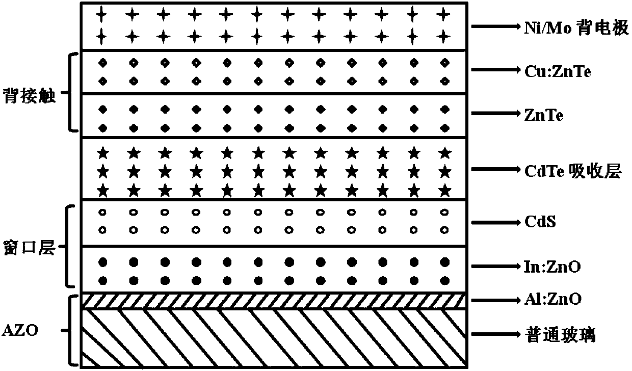
[0034] like figure 1As shown, a cadmium telluride thin-film battery with a composite window layer is sequentially provided with an aluminum-doped zinc oxide AZO glass substrate layer, an indium-doped zinc oxide window transition layer, a cadmium sulfide window layer, a cadmium telluride light-absorbing layer, and a telluride Zinc and copper-doped zinc telluride composite thin film back contact layer, nickel molybdenum thin film back electrode layer.
[0035] Among them, the thickness of the substrate layer is 50nm, the thickness of the indium-doped zinc oxide transition layer is 50nm, the thickness of the cadmium sulfide layer is 100nm, the thickness of the cadmium telluride thin film layer is 2μm, the thickness of the back contact layer is 20nm, and the thickness of the back electrode layer The thickness is 100nm.
[0036] The preparation method of the above-mentioned cadmium telluride thin film battery comprises the following steps:
[0037] (1) Use aluminum-zinc oxide-dop...
Embodiment 2
[0046] like figure 1 As shown, a cadmium telluride thin-film battery with a composite window layer is sequentially provided with an aluminum-doped zinc oxide AZO glass substrate layer, an indium-doped zinc oxide window transition layer, a cadmium sulfide window layer, a cadmium telluride light-absorbing layer, and a telluride Zinc and copper-doped zinc telluride composite thin film back contact layer, nickel molybdenum thin film back electrode layer.
[0047] Among them, the thickness of the substrate layer is 100nm, the thickness of the indium-doped zinc oxide transition layer is 100nm, the thickness of the cadmium sulfide layer is 200nm, the thickness of the cadmium telluride thin film layer is 3μm, the thickness of the back contact layer is 50nm, and the thickness of the back electrode layer The thickness is 200nm.
[0048] The preparation method of the above-mentioned cadmium telluride thin film battery comprises the following steps:
[0049] (1) Use AZO glass doped with...
PUM
 Abstract
Description
Claims
Application Information

