Trench-gate charge storage type IGBT and manufacturing method therefor

A technology of charge storage and trench gate, which is applied in semiconductor/solid-state device manufacturing, circuits, electrical components, etc., and can solve the problems affecting the compromise characteristics of device switching loss, the deterioration of device short-circuit safe working area, and the increase of device saturation current density, etc. problem, to achieve the effect of increasing the breakdown voltage, improving the carrier concentration distribution, and increasing the switching speed

Inactive Publication Date: 2018-03-06
UNIV OF ELECTRONICS SCI & TECH OF CHINA
View PDF10 Cites 14 Cited by
  • Summary
  • Abstract
  • Description
  • Claims
  • Application Information

AI Technical Summary

Problems solved by technology

[0005] The implementation of method (1) will increase the gate-emitter capacitance and gate-collector capacitance at the same time, and the switching process of the IGBT is essentially the process of charging / discharging the gate capacitance, so the increase in the gate capacitance will Makes the charging / discharging time longer, which in turn causes the switching speed to decrease
Therefore, the deep trench gate depth will reduce the switching speed of the device, increase the switching loss of the device, and affect the compromise characteristics of the device's conduction voltage drop and switching loss; and the implementation of method (2) will increase the device's switching loss The gate capacitance will reduce the switching speed of the device and increase the switching loss, which will affect the compromise between the conduction voltage drop and switching loss of the device. On the other hand, the large channel density will also increase the saturation current density of the device, making the device short-circuit safe. work area deterioration
In addition, the gate oxide layer in the trench gate structure is formed in the trench by one thermal oxidation. In order to ensure a certain threshold voltage, the thickness of the entire gate oxide layer is required to be small. However, the MOS capacitance and the thickness of the oxide layer Inversely proportional, which makes the thin gate oxide thickness in traditional CSTBT devices will significantly increase the gate capacitance of the device, and the electric field concentration effect at the bottom of the trench will reduce the breakdown voltage of the device, resulting in poor reliability of the device

Method used


Image

  • Trench-gate charge storage type IGBT and manufacturing method therefor
  • Trench-gate charge storage type IGBT and manufacturing method therefor
  • Trench-gate charge storage type IGBT and manufacturing method therefor

Examples


Embodiment 1

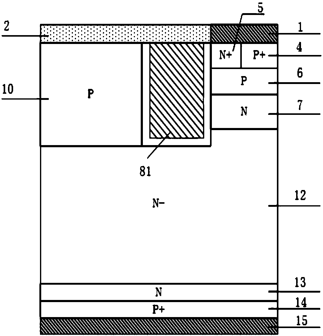
[0069] This embodiment provides a figure 2The trench gate charge storage type IGBT shown has a cellular structure including: a P-type collector region 14, a collector metal 15 on the back of the P-type collector region 14, and an N-type electric field on the front of the P-type collector region 14. The stop layer 13 and the N-type drift region 12 located above the N-type electric field stop layer 13; it is characterized in that: the N-type drift region 12 has a P+ emitter region 4, an N+ emitter region 5, a P-type base region 6, and an N-type charge storage Layer 7, trench gate structure, trench emitter structure, P-type body region 10 and P-type layer 11;

[0070] The trench emitter structure is located in the center of the top layer of the N-type drift region 12 and penetrates into it along the vertical direction of the device. The emitter dielectric layer 92 on the side of the trench emitter structure; the N-type drift region 12 on one side of the trench emitter structure...

Embodiment 2

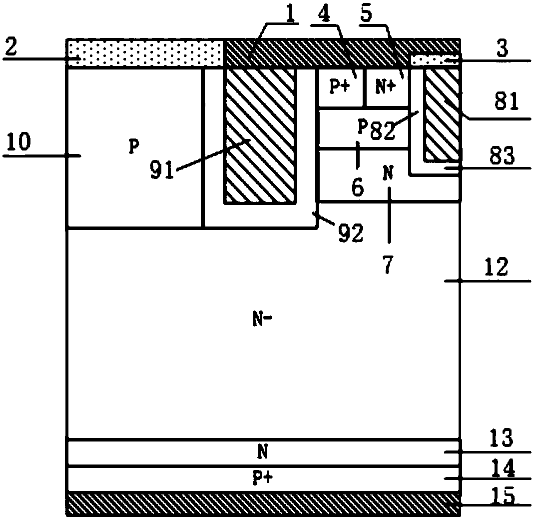
[0072] This embodiment provides a image 3 For the shown trench gate charge storage type IGBT, the present invention has the same structure as that of Embodiment 1 except that the first P-type layer 11 connected thereto is arranged under the trench emitter structure.

[0073] In this embodiment, by introducing the first P-type layer 11 connected to the trench emitter electrode 91 through the emitter dielectric layer 92 on the bottom side, the first P-type layer 11 extends laterally to one side to the bottom of the N-type charge storage layer 7 In the N-type drift region 12, the breakdown voltage of the device is improved, and at the same time, the contradiction between the breakdown voltage caused by the concentration of the charge storage layer and the forward conduction voltage drop is improved.

Embodiment 3

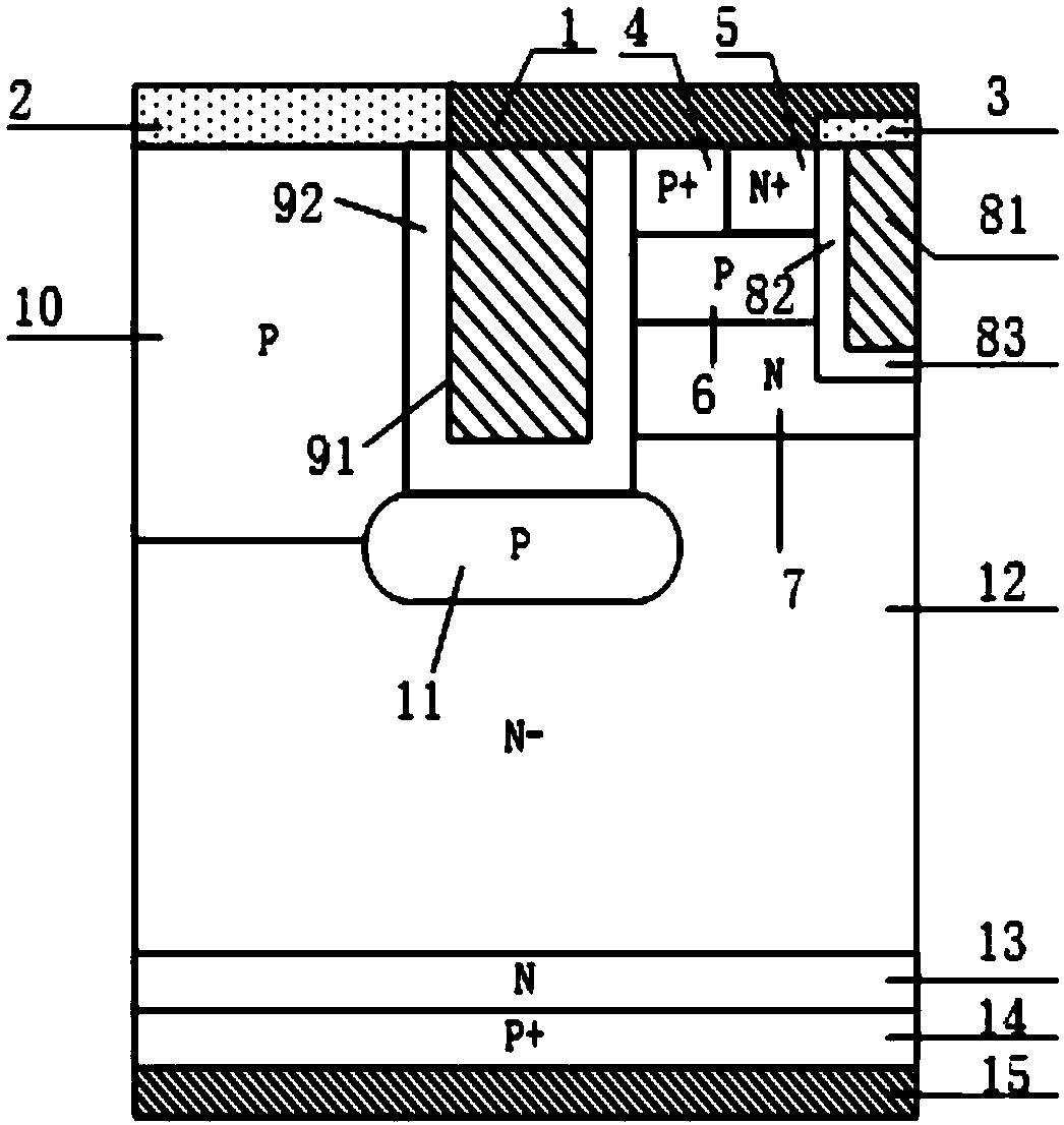
[0075] This embodiment provides a trench gate charge storage type IGBT, the cell structure of which is as follows Figure 4 As shown, the structure of this embodiment is the same as that of Embodiment 2 except that the second P-type layer 16 connected thereto is disposed under the trench gate structure.

[0076] This embodiment introduces the second P-type layer 16 connected to the gate electrode 81 through the bottom-side gate dielectric layer 83, and the second P-type layer 16 laterally extends to one side into the N-type drift region 12 below the N-type charge storage layer 7 , so as to shield the influence of negative charges in the N-type charge storage, reduce the gate capacitance, improve the concentration of the electric field at the bottom of the trench gate, and improve the breakdown voltage and reliability of the device.


PUM


Abstract

The invention discloses a trench-gate charge storage type IGBT and a manufacturing method therefor, and belongs to the technical field of semiconductor power devices. A trench-gate emitter structure connected with a P-type volume region is introduced to an N-type drift region at one side of a trench gate in a conventional CSTBT device, thereby enabling the gate-collector capacitance into gate-emitter capacitance, and improving the adverse effect of Miller capacitance. A thick dielectric layer of the trench-gate emitter structure avoids an electric field concentration effect at the bottom of atrench, and improves the breakdown voltage of a device. The depth of a gate electrode is enabled to be less than the junction depth of an N-type charge storage layer, thereby reducing the overall gatecapacitance under the condition that the connection of an IGBT is not affected, improving the switching speed of the device, reducing the switching loss of the device, and improving the compromise characteristics between a positive conduction voltage and the switching-off loss. According to the invention, the existing of the P-type volume region can reduce the extraction area of a hole, and improves the carrier concentration distribution of the whole N-type drift region. Moreover, the noise impact is reduced, and the EMI effect is avoided.

Description

technical field [0001] The invention belongs to the technical field of semiconductor power devices, in particular to an insulated gate bipolar transistor (IGBT), in particular to a trench gate charge storage type IGBT and a manufacturing method thereof. Background technique [0002] Insulated gate bipolar transistor (IGBT), as one of the core electronic components in modern power electronic circuits, is widely used in various fields such as transportation, communication, household appliances, and aerospace. Insulated gate bipolar transistor (IGBT) is a new type of power electronic device composed of an insulated field effect transistor (MOSFET) and a bipolar junction transistor (BJT), which can be equivalent to a MOSFET driven by a bipolar junction transistor. . IGBT combines the working mechanism of MOSFET structure and bipolar junction transistor. It not only has the advantages of MOSFET easy to drive, low input impedance, and fast switching speed, but also has the advant...

Claims


Application Information

Patent Timeline
Patent Type & Authority Applications(China)
IPC IPC(8): H01L29/739H01L29/08H01L29/06H01L21/331
CPCH01L29/0649H01L29/0657H01L29/0804H01L29/66348H01L29/7397
Inventor 张金平赵倩刘竞秀李泽宏任敏张波
Owner UNIV OF ELECTRONICS SCI & TECH OF CHINA
Why Eureka
Try Eureka