Forming method and forming device of perovskite layer film and use method and application thereof

A molding method and molding equipment technology, applied in coating, metal material coating process, gaseous chemical plating and other directions, can solve the problems of affecting film properties, unable to achieve continuous production, film properties differences, etc., to improve production efficiency Effect

Pending Publication Date: 2018-03-09
HANGZHOU MICROQUANTA SEMICON CO LTD
View PDF4 Cites 3 Cited by
  • Summary
  • Abstract
  • Description
  • Claims
  • Application Information

AI Technical Summary

Problems solved by technology

The existing low-pressure chemical vapor deposition (LPCVD) method requires auxiliary gas during the deposition process, and the vaporized nitrogen-containing organic salt halide (AX) is deposited unevenly during the reaction process, and the placement of the substrate will greatly affect the properties of the film , so that the properties of the films prepared in the same batch are different; at the same time, annealing or solvent-assisted annealing process cannot be performed immediately after film formation, and continuous production cannot be realized

Method used


Image

  • Forming method and forming device of perovskite layer film and use method and application thereof
  • Forming method and forming device of perovskite layer film and use method and application thereof
  • Forming method and forming device of perovskite layer film and use method and application thereof

Examples


Embodiment 1

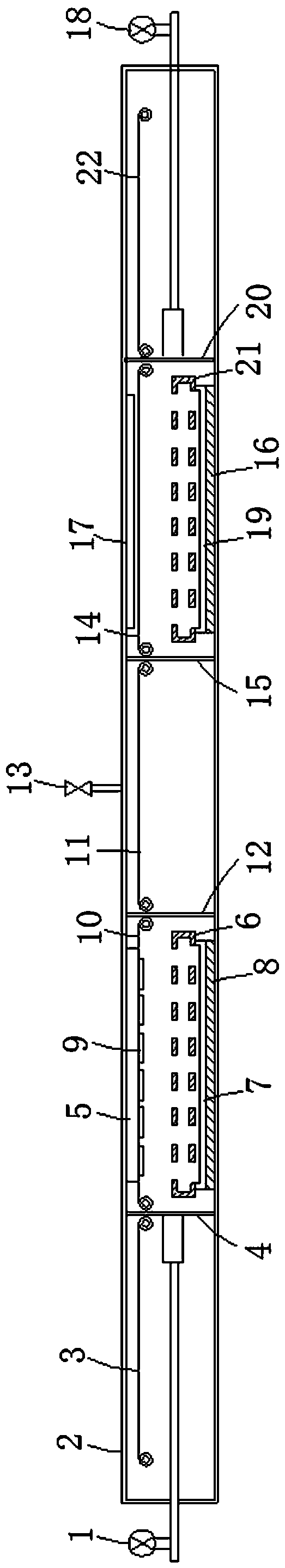
[0065] Please refer to Figure 7 As shown, the application of the forming equipment of the perovskite layer thin film of the present invention in the field of making solar cells specifically includes the following steps:

[0066] (1) Clean an ITO glass plate of 2.5×2.5cm by ultrasonic cleaning for 30 minutes with detergent, deionized water, acetone and isopropanol, and then use N 2 After drying, it was treated with UV O-zone for 10 minutes;

[0067] (2) Spin-coat PEDOT:PSS, dry at 90°C~150°C for 5min~20min;

[0068] (3) PbBr 2 Dissolve in DMF with a concentration of 1M, stir at 70°C for 2h, and spin-coat PEDOT:PSS to obtain PbBr 2 For thin film, anneal at 70℃~100℃ for 5min~60min;

[0069] (4) will be deposited with the precursor PbBr 2 One or more substrates 9 are placed on the substrate frame 24, the partition 4 is opened, and the substrate is transported to the deposition chamber M2 through the substrate entering chamber M1 through the conveying device 3 and 10, and the...

Embodiment 2

[0080] The molding equipment of the perovskite layer thin film of the present invention is applied in the field of making LED, specifically comprises the following steps:

[0081] (1) Clean the 2.5×2.5cm FTO ethylene glycol phthalate board with detergent, deionized water, acetone, and isopropanol for 20 minutes, and then use N 2 After drying, it was treated with UV O-zone for 15 minutes;

[0082] (2) Spin-coat CuSCN and dry at 100°C~200°C for 5min~20min;

[0083] (3) PbCl 2 Dissolve in DMF with a concentration of 1M, stir at 70°C for 2h, and spin-coat CuSCN to obtain PbCl 2 For thin film, anneal at 70℃~100℃ for 5min~60min;

[0084] (4) will be deposited with the precursor PbBr 2 One or more substrates 9 are placed on the substrate frame 24, the partition 4 is opened, and the substrate is transported to the deposition chamber M2 through the substrate entering chamber M1 through the conveying device 3 and 10, and the partition 4 is closed;

[0085] (5) Open the partition 12...

Embodiment 3

[0092] The forming equipment of the perovskite layer thin film of the present invention is applied in the field of making thin film field effect tubes, specifically comprises the following steps:

[0093] (1) Clean an ITO glass plate of 2.5×2.5cm by ultrasonic cleaning for 30 minutes with detergent, deionized water, acetone and isopropanol, and then use N 2 After drying, it was treated with UV O-zone for 10 minutes;

[0094] (2) Spin-coat PEDOT:PSS, dry at 90°C~150°C for 5min~20min;

[0095] (3) PbBr 2 Dissolve in DMF with a concentration of 1M, stir at 70°C for 2h, and spin-coat PEDOT:PSS to obtain PbBr 2 For thin film, anneal at 70℃~100℃ for 5min~60min;

[0096] (4) will be deposited with the precursor PbBr 2 One or more substrates 9 are placed on the substrate frame 24, the partition 4 is opened, and the substrate is transported to the deposition chamber M2 through the substrate entering chamber M1 through the conveying device 3 and 10, and the partition 4 is closed;

...


PUM

PropertyMeasurementUnit
sizeaaaaaaaaaa

Abstract

The invention relates to a forming method and forming device of a perovskite layer film and a use method and application thereof. The forming method is characterized in that a tubular cavity is sequentially provided with five parts including a substrate entering section, a depositing cavity, a transition cavity, an annealing section and a substrate removing section, wherein a conveying device is arranged in the tubular cavity; a loading platform, an air pressure regulating device and a heating device are correspondingly arranged in the depositing cavity and the annealing cavity; adjacent sections are separated from the cavity through separating plates, and the cavities are separated through the separating plate; the substrate to be deposited with the film is positioned on a substrate rackand sequentially continuously passes through the depositing cavity, the transition cavity and the annealing cavity from the substrate entering section through the conveying device; then the substrateon which a perovskite layer film is deposited is removed from the substrate rack in the substrate removing section. According to the method, the depositing filming and the annealing technology are integrated to realize the continuous production of the perovskite layer film product. The perovskite layer film manufactured through the device is uniform in crystal particle size, design in crystal particle, and high in photoelectric conversion efficiency.

Description

technical field [0001] The invention belongs to the technical field of perovskite layer thin films, and in particular relates to a forming method, forming equipment, and use methods and applications of perovskite layer thin films. Background technique [0002] A solar cell is a photoelectric conversion device that uses the photovoltaic effect of semiconductors to convert solar energy into electrical energy. So far, solar power has become the most important renewable energy besides hydropower and wind power. The semiconductors currently used for commercialization include monocrystalline silicon, polycrystalline silicon, amorphous silicon, cadmium telluride, copper indium gallium selenide, etc., but most of them consume a lot of energy and cost. [0003] In recent years, a perovskite solar cell that uses organometallic halides as the light absorbing layer has received much attention. Perovskite as ABX 3 type of cubo-octahedral structure, such as figure 1 shown. The thin...

Claims


Application Information

Patent Timeline
Patent Type & Authority Applications(China)
IPC IPC(8): C23C16/458C23C16/56
CPCC23C16/458C23C16/56
Inventor 姚冀众颜步一
Owner HANGZHOU MICROQUANTA SEMICON CO LTD
Why Eureka
Try Eureka