
Multi-beam type single-mass block in-plane biaxial acceleration sensor chip and preparation method thereof
A dual-axis acceleration, sensor chip technology, applied in the direction of acceleration measurement using inertial force, can solve the problems of being easily affected by parasitic capacitance, narrow frequency response range, low sensitivity, etc., to improve dynamic performance and application range, reduce Interference of cross-sensitivity and the effect of alleviating conflicting relationships
- Summary
- Abstract
- Description
- Claims
- Application Information
AI Technical Summary
Problems solved by technology
Method used
Image

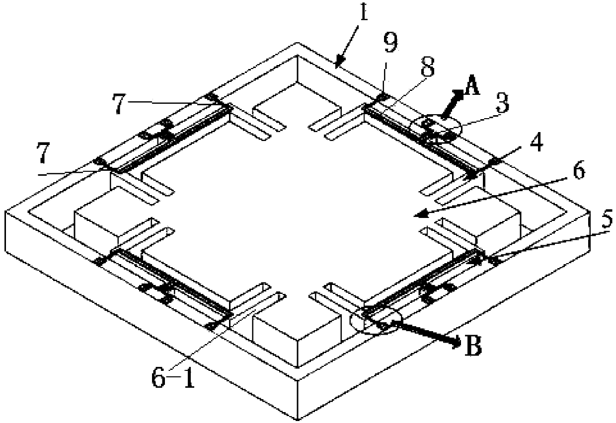
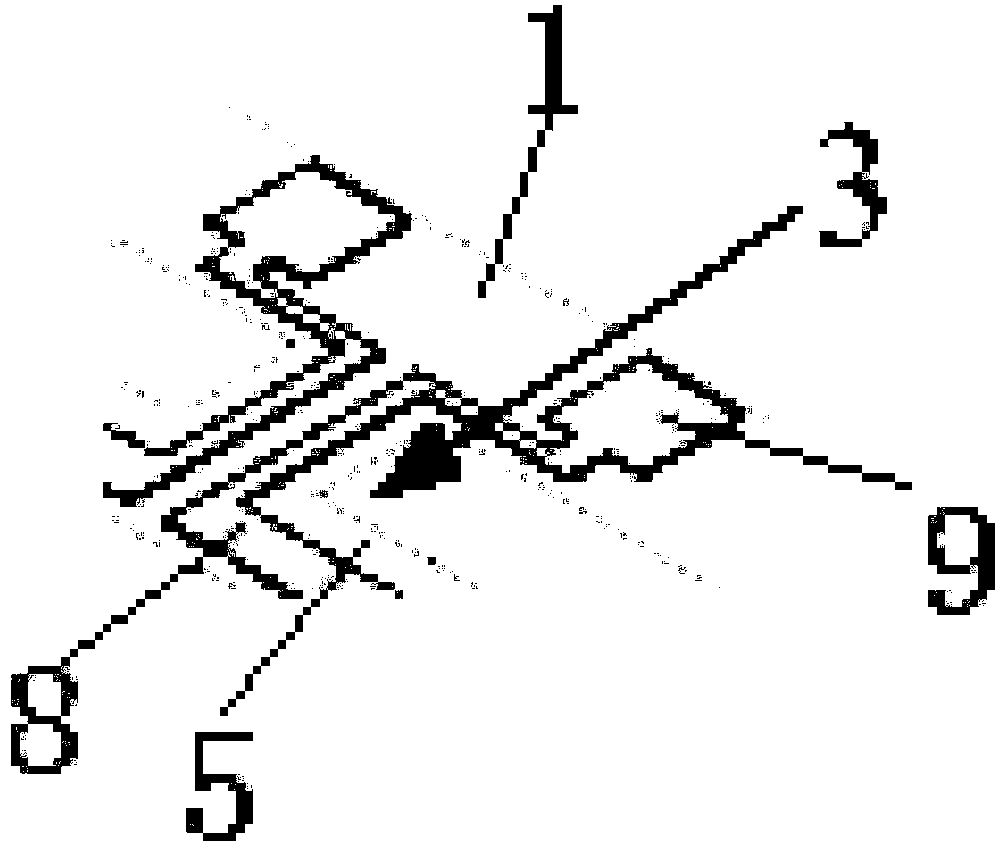
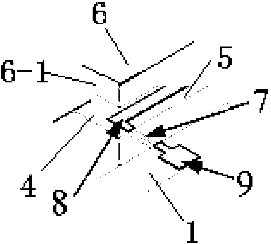
Examples
Embodiment
[0070] The method for preparing the acceleration sensor chip of the present embodiment comprises the following steps, referring to Figure 6 to Figure 8 :
[0071] Step 1), use the HF solution with a volume concentration of 49% to clean the SOI silicon chip of the N-type (100) crystal plane; the structure of the SOI silicon chip from top to bottom is: The layer 14 and the lower layer of single crystal silicon 15 have a thickness of 10 μm, 1 μm and 304 μm in sequence, wherein the buried silicon dioxide layer 14 separates the upper layer of single crystal silicon 13 from the lower layer of single crystal silicon 15;
[0072] Step 2), then carry out high-temperature oxidation on the SOI silicon wafer, the oxidation temperature is 900-1200 ° C, and form a silicon dioxide layer 10 on the front and back sides of the SOI silicon wafer, and then use a P-varistor plate to oxidize the upper layer single crystal The silicon dioxide layer 10 formed on the surface of the silicon 13 is pho...
PUM
| Property | Measurement | Unit |
|---|---|---|
| Sheet resistance | aaaaa | aaaaa |
| Sheet resistance | aaaaa | aaaaa |
| Sensitivity | aaaaa | aaaaa |
Abstract
Description
Claims
Application Information