Black silicon and preparation process, and preparation method for black silicon-based MEMS device

A preparation process, black silicon technology, applied in the nanometer field, can solve problems such as damage and inability to achieve protection, and achieve the effects of avoiding damage, fast large-scale batch processing, and improving light absorption capacity

Active Publication Date: 2018-03-13
INST OF MICROELECTRONICS CHINESE ACAD OF SCI
View PDF6 Cites 6 Cited by
  • Summary
  • Abstract
  • Description
  • Claims
  • Application Information

AI Technical Summary

Problems solved by technology

However, black silicon still has the physical and chemical properties of silicon materials, so it is easily damaged by corrosive gases or corrosive liquids in the subsequent release process; and beca

Method used


Image

  • Black silicon and preparation process, and preparation method for black silicon-based MEMS device
  • Black silicon and preparation process, and preparation method for black silicon-based MEMS device
  • Black silicon and preparation process, and preparation method for black silicon-based MEMS device

Examples


no. 1 example

[0053] The present disclosure provides a process for preparing black silicon, including the following steps:

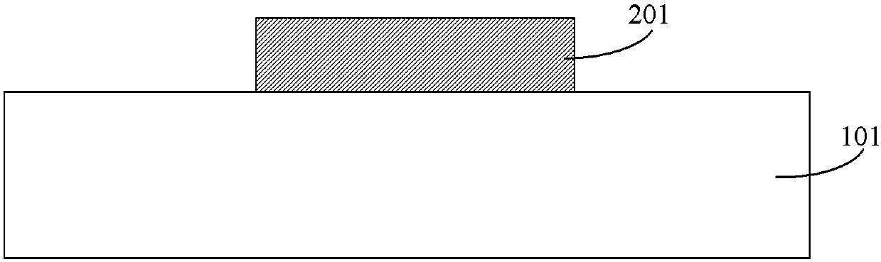
[0054] Step A1: such as figure 1 As shown, a substrate 101 is provided.

[0055] Further, the substrate includes silicon, glass, quartz, and polymer; the substrate is not limited to the above four types, and may be any substrate commonly used in microelectronics technology. The substrate can be a 4-inch, 6-inch, 8-inch, 12-inch wafer, and other substrate sheets of different shapes and sizes suitable for micromachining processes.

[0056] In this embodiment, a 4-inch monocrystalline silicon substrate is used.

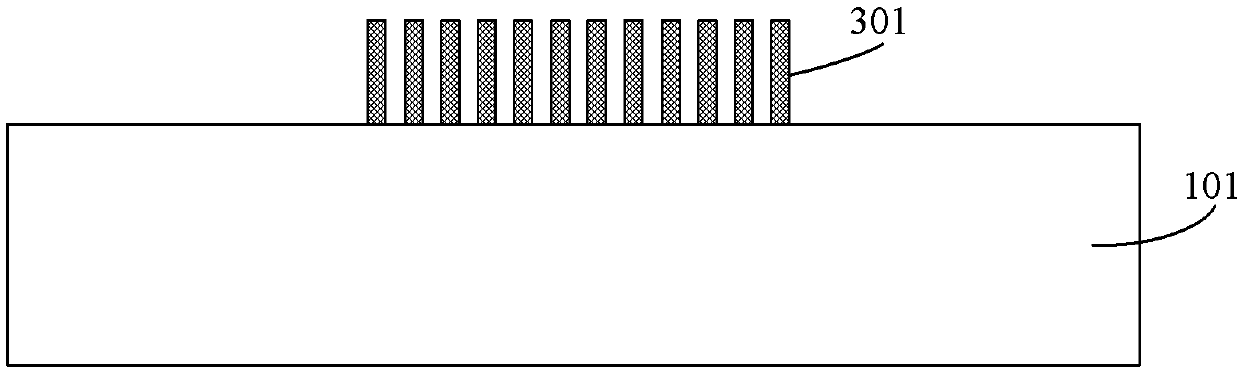
[0057] Step A2: forming a polymer layer 201 on the substrate 101.

[0058] Further, the material of the polymer layer includes photoresist, polydimethylsiloxane, parylene, polyethylene, polycarbonate, and other polymer layers that can be removed by plasma bombardment. material;

[0059] The polymer layer may be disposed on the substrate 101 by spraying, spin coating, pas...

no. 3 example

[0106] The difference between the black silicon-based MEMS device manufacturing method provided in this embodiment and the second embodiment is that this embodiment uses a front release process to corrode the substrate to form the back corrosion cavity of the MEMS sensor. The method includes the following steps:

[0107] Step C1 to Step C3 are the same as Step B1 to Step B3.

[0108] Step C4: such as Figure 13 As shown, a front corrosion release hole 501 is provided on the polymer layer, the sensor sensitive structure, and the sensor base structure.

[0109] Further, the front side corrosion release hole is prepared by a photolithography or etching process, and the front side corrosion release hole penetrates the patterned polymer layer, the sensor sensitive structure and the sensor basic structure, and is connected to the substrate 102.

[0110] Step C5: Such as Figure 14 As shown, the front side dry etching is used to perform the front side etching release of the substrate 102 to f...


PUM

PropertyMeasurementUnit
Thicknessaaaaaaaaaa
Diameteraaaaaaaaaa
Heightaaaaaaaaaa

Abstract

The invention provides a black silicon preparation process. The preparation process comprises the steps of forming a polymer layer on a substrate; removing the polymer layer, and forming a nanometer forest structure at the initial position of the polymer layer by the product generated in the polymer layer removal process; and depositing a silicon thin film material layer on the nanometer forest structure to complete black silicon preparation. The invention also provides black silicon prepared by the black silicon preparation process, and a preparation method of a black silicon-based MEMS device. By virtue of the black silicon, the preparation process, and the preparation method of the black silicon-based MEMS device disclosed in the invention, the black silicon with higher optical absorption capability is prepared by the black silicon preparation process with low process cost and high popularity and adaptation; and in addition, by adoption of the preparation method of the black silicon-based MEMS device, corrosion damage to the black silicon in the releasing process of the MEMS device is avoided.

Description

Technical field [0001] The present disclosure belongs to the field of nanotechnology, and in particular relates to a black silicon, a preparation process and a preparation method of a MEMS device based on black silicon. Background technique [0002] Black silicon is a large-area nano-pillar / needle structure in the shape of a forest. It was once considered a revolutionary new material in the electronics industry. Compared with traditional silicon materials, black silicon has a very high absorption efficiency for light from visible light to near-infrared. Various methods have been proposed for preparing black silicon, including high-energy femtosecond laser-assisted etching, metal-catalyzed electrochemical etching, and plasma dry etching. Due to the comprehensive consideration of processing cost, process convenience and process compatibility, the method of preparing black silicon by plasma dry etching technology is most commonly used in conventional semiconductor processes, but th...

Claims


Application Information

Patent Timeline
IPC IPC(8): H01L21/02B81B7/02B81C1/00B82Y30/00
CPCB81B7/02B81C1/00349B82Y30/00H01L21/02532H01L21/02592H01L21/02595H01L21/02598
Inventor 毛海央杨宇东
Owner INST OF MICROELECTRONICS CHINESE ACAD OF SCI
Why Eureka
Try Eureka