Etching method of grooves in wafer

A technology of grooves and wafers, which is applied in the direction of electrical components, semiconductor/solid-state device manufacturing, circuits, etc., can solve the problems of residual, deep groove edge morphology that is easily affected by process fluctuations, etc., and achieves improved yield and is not easy Breakdown, the effect of accelerating the reaction rate

Inactive Publication Date: 2018-04-06
YANGZHOU YANGJIE ELECTRONIC TECH CO LTD
View PDF5 Cites 0 Cited by
  • Summary
  • Abstract
  • Description
  • Claims
  • Application Information

AI Technical Summary

Problems solved by technology

This will have a certain impact on the subsequent silicon chemical mechanical polishing process. It is difficult for the polishing pad to contact the recessed area, resulting in residue
[0005] In addition, when the oxide film-nitride film-oxide film structure is used as an etching barrier layer, when the oxide film on the surface is removed after the etching is completed, the part of the underlying oxide film close to the deep trench will also be subjected to lateral erosion, and the deep trench Groove edge topography is susceptible to process fluctuations

Method used


Image

  • Etching method of grooves in wafer
  • Etching method of grooves in wafer
  • Etching method of grooves in wafer

Examples


Embodiment Construction

[0031] The present invention as Figure 1-5 shown, including the following steps:

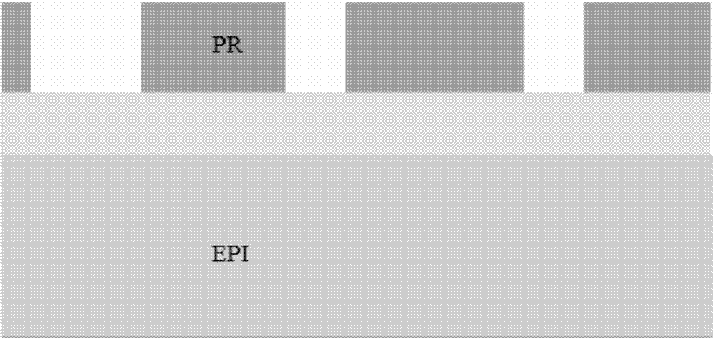
[0032] 1) Deposit a hard mask layer (LPTEOS) on the surface of the silicon body;

[0033] 2) Make a photomask on the hard mask, and use a protective layer (PR, photomask) to block the places that do not need to be etched;

[0034] 3) Etching is performed in the area without the protective layer until the surface of the silicon body (EPI) is exposed;

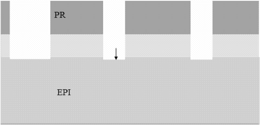
[0035] 4) Remove the photomask on the surface of the silicon body and clean it to obtain a clean surface;

[0036] 5) Use the hard mask layer as the barrier layer to etch the silicon body to obtain the required deep trench;

[0037] The specific steps of etching the silicon body in the step 5) are:

[0038] 5.1) Remove the natural oxide layer on the surface of the silicon body; a layer of natural oxide layer will be formed after the silicon body is in contact with air, which will reduce the etching efficiency, so it needs to be removed.

[00...


PUM


Abstract

The invention provides an etching method of grooves in a wafer, relates to a wafer processing technology, in particular to an etching method of the grooves in the wafer. According to the provided method of the grooves in the wafer, the bottom surfaces of the grooves are smooth, a growing oxide layer is uniform, and a cavity is clean and the using period is long in the etching process. The method comprises the following steps: (1) depositing a hard mask layer on the surface of a silicon body; (2) carrying out photomasking on the hard mark, wherein the part without the need of etching is blockedwith a protective layer; (3) etching an area without the protective layer until the surface of the silicon body is exposed; (4) removing the mask on the surface of the silicon body, and cleaning thesilicon body to obtain a clean surface; and (5) using the hard mask as a blocking layer, and etching the silicon body to obtain the grooves with required depths. According to the method, clean and tidy cavity for etching is guaranteed, the using period is long, the etching efficiency can be quickened, and sediments can be prevented from being sedimented inside the cavity and the grooves to influence the performance.

Description

technical field [0001] The invention relates to a wafer processing technology, in particular to a method for etching grooves on a wafer. Background technique [0002] Trench structures are widely used in today's semiconductor technology. For example, trenches can be used as isolation structures to isolate electronic devices operating at different voltages. Applying it to the silicon germanium bipolar complementary metal oxide semiconductor process can reduce the capacitance of the substrate NPN transistor and improve the frequency characteristics of the device. As another example, deep trenches can be applied to super junction MOS transistors, as a PN junction achieves high breakdown voltage performance through charge balance in the depletion state. [0003] At present, the method of etching and filling deep trenches in the manufacturing process of super junction MOS transistors is to grow an n-type epitaxial layer (single crystal silicon) on a p-type silicon substrate, an...

Claims


Application Information

Patent Timeline
Patent Type & Authority Applications(China)
IPC IPC(8): H01L21/306H01L21/308
CPCH01L21/30604H01L21/3081H01L21/3086
Inventor 丁佳曹俊蒋方圆王毅
Owner YANGZHOU YANGJIE ELECTRONIC TECH CO LTD
Why Eureka
Try Eureka