
1P2M CMOS packaging method

An encapsulation method and passivation layer technology, which are applied to electrical components, electrical solid-state devices, circuits, etc., can solve the problems of long operation time and high material cost, and achieve the effect of saving operation time, material cost and good application prospect.

Inactive Publication Date: 2018-04-13
NINGBO CHIPEX SEMICON
View PDF3 Cites 2 Cited by
  • Summary
  • Abstract
  • Description
  • Claims
  • Application Information

AI Technical Summary

Problems solved by technology

[0002] 2P2M and 1P2M are a technology that grows the bumps at the proper position of the chip through rewiring. Compared with 1P2M, 2P2M has an extra layer of PI and an extra layer of copper and titanium sputtering, which leads to more material costs and longer operating time.

Method used


Image

  • 1P2M CMOS packaging method
  • 1P2M CMOS packaging method
  • 1P2M CMOS packaging method

Examples


Embodiment 1

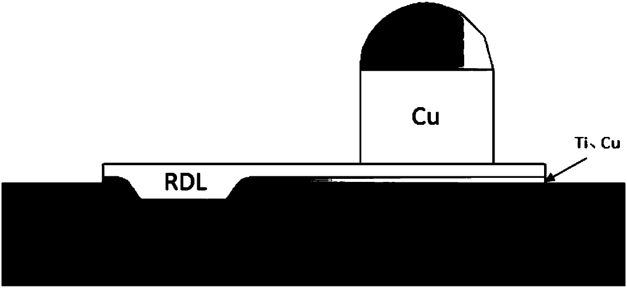
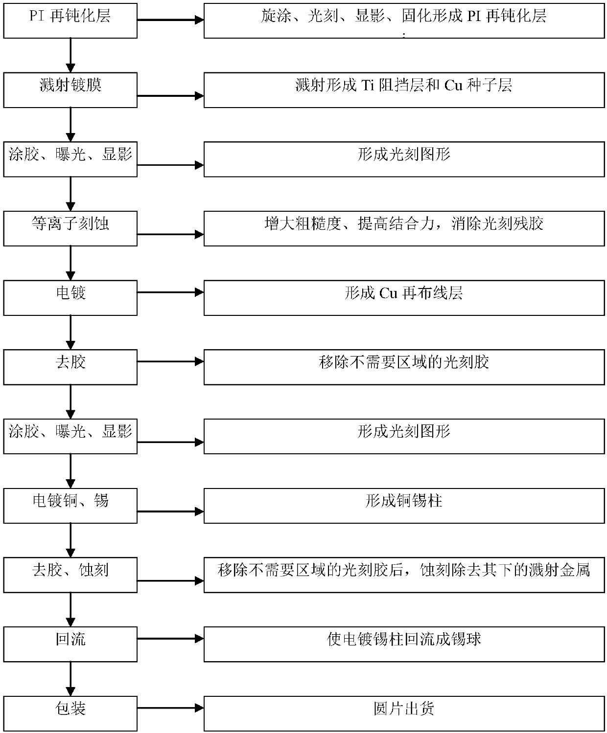
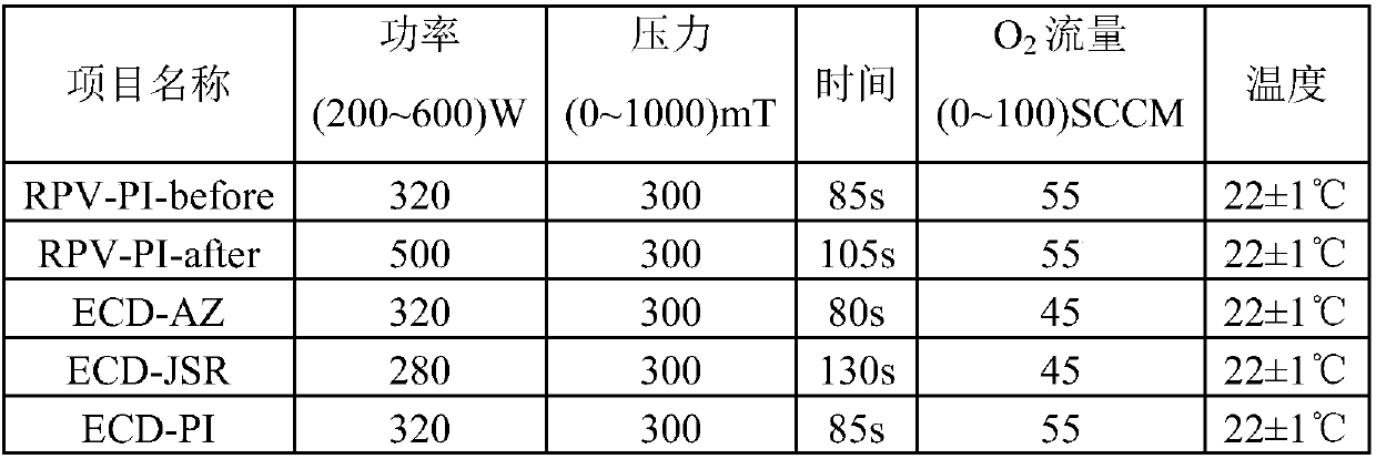
[0024] 1) Multi-layer polyimide (PI) passivation layer coating process

[0025] Polyimide (PI) photoresist has outstanding heat resistance, excellent mechanical properties, insulation and corrosion resistance. First, the automatic coating machine quantitatively coats 5ml of PI glue on the surface of the wafer, and finally forms a layer of 5um polyimide re-passivation layer on the surface of the wafer through spin coating, pre-baking, photolithography, development and curing processes , play the role of insulation, corrosion resistance, stress buffer and planarization. Among them, spin coating is divided into uniform glue (200±20rpm, 7±1s), spin glue (2450±100rpm, 30±3s), BSR (1000±50rpm, 15±1s), spin dry (1000±50rpm, 10±1s) ), side throwing (3000±50rpm, 1±0.1s) 5 processes, stepper exposure is carried out under the exposure energy of 300mj and the spacing of 4um after the coating is completed, and the developer is KS5400 (Shanghai Feikai Optoelectronic Materials Co., Ltd.) D...


PUM

PropertyMeasurementUnit
Thicknessaaaaaaaaaa

Abstract

The invention relates to a 1P2M CMOS packaging method, which comprises the procedures of photoetching, sputtering, plasma etching, electroplating, photoresist removing, refluxing and the like. According to the packaging, 1P2M does not have a second PI layer relative to 2P2M, a first Ti, Cu sputtering layer is not required to be etched, and a second Ti, Cu layer is not required to be sputtered, thereby being still capable of keeping the due performance while more saving the raw material cost and the working time, and having good application prospects.

Description

technical field [0001] The invention belongs to the field of wafer-level chip packaging, in particular to a 1P2M CMOS packaging method. Background technique [0002] 2P2M and 1P2M are a technology that grows the bumps at the proper position of the chip through rewiring. Compared with 1P2M, 2P2M has an extra layer of PI and an extra layer of copper and titanium sputtering. The material cost is more and the operation time is longer. Contents of the invention [0003] The technical problem to be solved by the present invention is to provide a 1P2M CMOS packaging method, the 1P2M packaged by this method has less second layer PI than 2P2M, no need to etch the first Ti, Cu sputtering layer, no need to sputter the second layer Ti and Cu, while saving raw material costs and working time, can still maintain their proper performance and have good application prospects. [0004] The invention provides a 1P2M CMOS packaging method, including: [0005] (1) Coating a polyimide passiva...

Claims


Application Information

Patent Timeline
IPC IPC(8): H01L23/31H01L23/498H01L21/56
CPCH01L2224/11H01L23/3121H01L21/561H01L23/3128H01L23/49816H01L23/49827
Inventor 于政方梁洪罗立辉蓝敏华
Owner NINGBO CHIPEX SEMICON
Features
  • Generate Ideas
  • Intellectual Property
  • Life Sciences
  • Materials
  • Tech Scout
  • Unparalleled Data Quality
  • Higher Quality Content
  • 60% Fewer Hallucinations
Learn More