Capacitor array structure and manufacture method thereof

A technology of array structure and manufacturing method, which is applied in the direction of capacitors, electric solid devices, circuits, etc., can solve the problems of affecting the performance, the conductivity of the capacitor medium layer increases the leakage current, and the presence of bubbles, so as to reduce the impact, reduce the formation process temperature, Effect of increasing movement speed

Pending Publication Date: 2018-04-13
CHANGXIN MEMORY TECH INC
View PDF8 Cites 25 Cited by
  • Summary
  • Abstract
  • Description
  • Claims
  • Application Information

AI Technical Summary

Problems solved by technology

[0004] In view of the above-mentioned shortcomings of the prior art, the object of the present invention is to provide a capacitor array structure and its manufacturing method, which is used to solve the problem of excessive crystallization of the capacitor dielectric layer caused by the high process temperature of the filling lay

Method used


Image

  • Capacitor array structure and manufacture method thereof
  • Capacitor array structure and manufacture method thereof
  • Capacitor array structure and manufacture method thereof

Examples


Embodiment 1

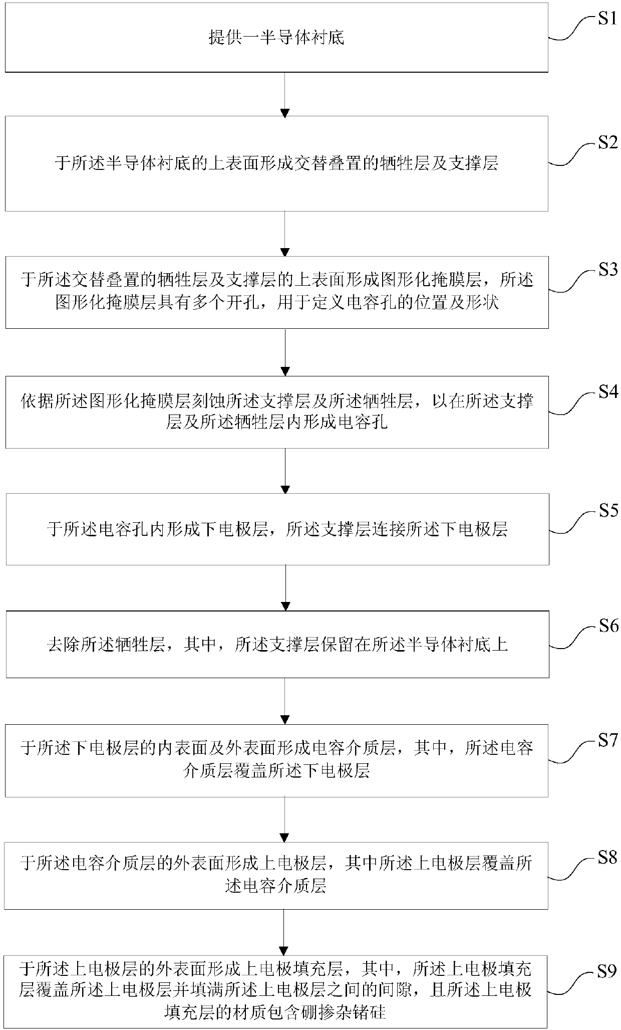
[0080] See figure 1 This embodiment provides a method for manufacturing a capacitor array structure. The method for manufacturing the capacitor array structure includes the following steps:

[0081] 1) Provide a semiconductor substrate;

[0082] 2) Forming alternately stacked sacrificial layers and supporting layers on the upper surface of the semiconductor substrate;

[0083] 3) forming a patterned mask layer on the upper surface of the alternately stacked sacrificial layer and support layer, the patterned mask layer having a plurality of openings for defining the position and shape of the capacitor hole;

[0084] 4) Etching the support layer and the sacrificial layer according to the patterned mask layer to form capacitor holes in the support layer and the sacrificial layer;

[0085] 5) forming a lower electrode layer in the capacitor hole, and the support layer is connected to the lower electrode layer;

[0086] 6) removing the sacrificial layer, wherein the supporting layer remains o...

Embodiment 2

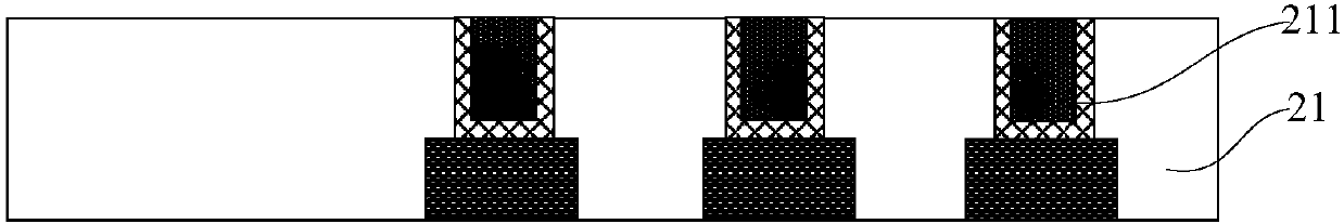
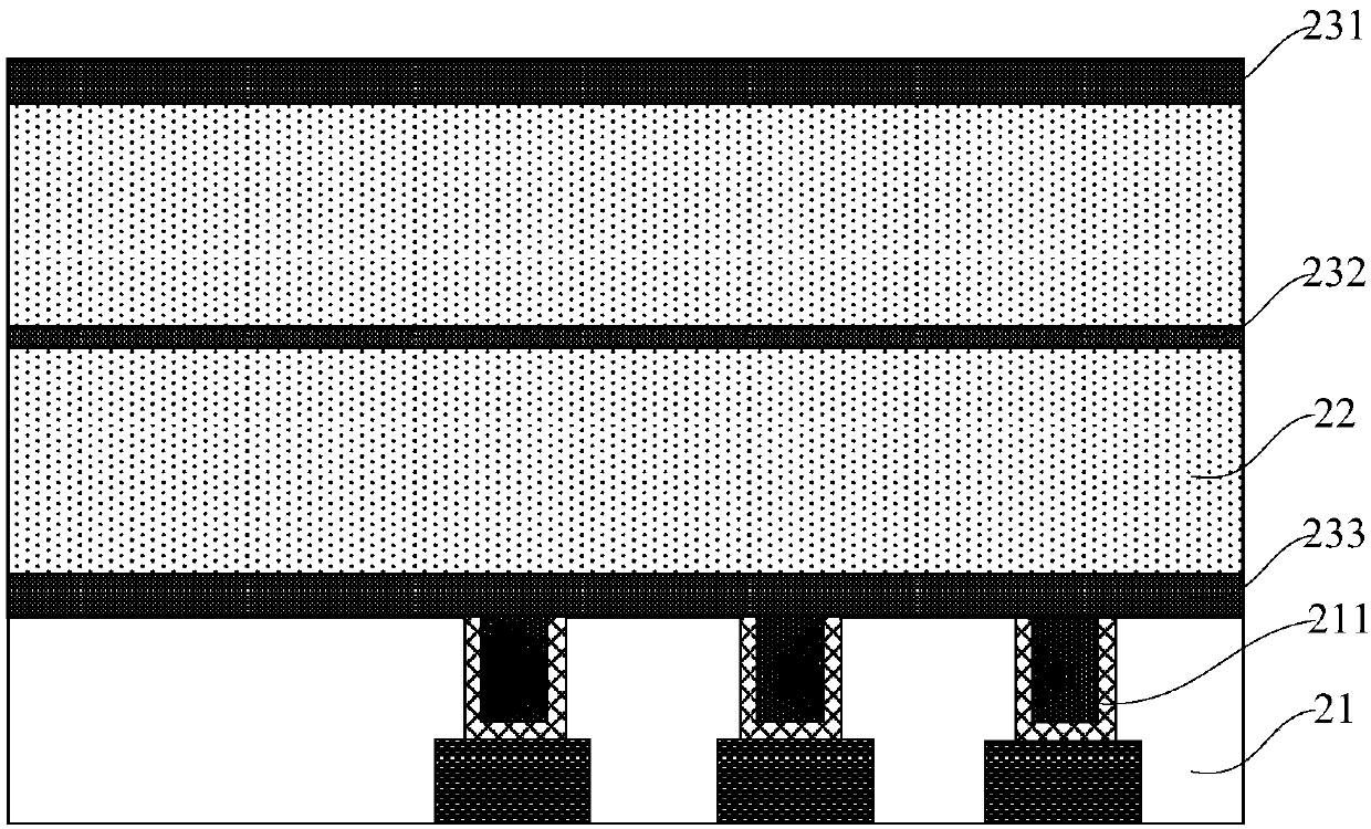
[0136] Please continue to refer to Example 1 Figure 13 This embodiment also provides a capacitor array structure which is manufactured by the manufacturing method described in the first embodiment, the capacitor array structure is disposed on the semiconductor substrate 21, and the semiconductor substrate 21 A plurality of pads 211 in a memory array structure are formed thereon. The capacitor array structure includes a lower electrode layer 26, the lower electrode layer 26 is bonded to the pad 211, and the cross-sectional shape of the lower electrode layer 26 U-shaped; the capacitor dielectric layer 27, the capacitor dielectric layer 27 covers the inner and outer surfaces of the lower electrode layer 26; the upper electrode layer 28, the upper electrode layer 28 covers the capacitor dielectric layer 27 The outer surface; the upper electrode filling layer 29, the upper electrode filling layer 29 covers the outer surface of the upper electrode layer 28, and fills the gap between...

Embodiment 3

[0153] This embodiment also provides a semiconductor storage device structure. The semiconductor storage device structure includes the capacitor array structure described in the second embodiment. For the specific structure of the capacitor array structure, please refer to the second embodiment. Narrated.

[0154] As an example, the structure of the semiconductor memory device may be, but is not limited to, a dynamic random access memory (DRAM).

[0155] In summary, the capacitor array structure and the manufacturing method thereof of the present invention include the following steps: 1) providing a semiconductor substrate; 2) forming alternate stacks on the upper surface of the semiconductor substrate 3) A patterned mask layer is formed on the upper surface of the alternately stacked sacrificial layer and the support layer. The patterned mask layer has a plurality of openings for defining capacitor holes 4) etching the support layer and the sacrificial layer according to the patt...


PUM

PropertyMeasurementUnit
Thicknessaaaaaaaaaa
Thicknessaaaaaaaaaa

Abstract

The invention provides a capacitor array structure and a manufacture method thereof. The method includes 1) providing a semiconductor substrate; 2) forming sacrificial layer and support layers in an alternating and stacking manner on the upper surface of the semiconductor substrate; 3) forming graphic mask layers on the upper surfaces of the sacrificial layer and support layers arranged in an alternating and stacking manner, wherein the graphic mask layers have a plurality of holes; 4) forming capacitance holes in the support layers and the sacrificial layers; 5) forming lower electrode layersin the capacitance layers; 6) removing the sacrificial layers and remaining the support layers on the semiconductor substrate; 7) forming capacitance medium layers on the inner surfaces and the outersurface of the lower electrode layers; 8) forming upper electrode layers on the outer surfaces of the capacitance medium layers; 9) forming upper electrode filling layers on the outer surface of theupper electrode layers, wherein the material of the upper electrode filling layers contains boron doped germanium-silicon. According to the invention, temperature of a formation technique can be reduced, so that influence on the capacitance medium layers by thermal budge can be reduced. At the same time, current carrier moving rate can be improved, so that the resistance value of the filling layers can be reduced.

Description

Technical field [0001] The invention belongs to the field of semiconductor devices and manufacturing, and particularly relates to a capacitor array structure and a manufacturing method thereof. Background technique [0002] Dynamic random access memory (Dynamic Random Access Memory, referred to as: DRAM) is a semiconductor storage device commonly used in computers, which is composed of many repeated storage units. In the DRAM manufacturing process below 20nm, DRAM adopts a stacked capacitor structure. The capacitor is a vertical cylindrical shape with a high aspect ratio to increase the surface area. Therefore, it must include the lower electrode layer, the capacitor dielectric layer and the upper electrode layer. The capacitor gap of the electrode layer is filled with a filling layer to stabilize the capacitor structure. [0003] Since the capacitor dielectric layer of the capacitor is greatly affected by the thermal budget, if the filling layer uses a high-temperature process, t...

Claims


Application Information

Patent Timeline
IPC IPC(8): H01L27/108H01L23/64
CPCH01L28/40H01L28/75H10B12/20
Inventor 不公告发明人
Owner CHANGXIN MEMORY TECH INC
Why Eureka
Try Eureka