Transverse high-voltage bipolar junction transistor and manufacturing method thereof

A bipolar junction, lateral high-voltage technology, applied in semiconductor/solid-state device manufacturing, semiconductor devices, electrical components, etc., can solve problems such as large leakage and insufficient withstand voltage of lateral high-voltage bipolar junction transistors, and achieve the curvature effect. The effect of reducing and reducing leakage current

Pending Publication Date: 2018-04-20
CHONGQING ZHONGKE YUXIN ELECTRONICS
View PDF0 Cites 5 Cited by
  • Summary
  • Abstract
  • Description
  • Claims
  • Application Information

AI Technical Summary

Problems solved by technology

[0005] The purpose of the present invention is to solve the problems of insufficient withstand voltage and large leakage of lateral high-voltage bipolar junction transistors in the prior art

Method used


Image

  • Transverse high-voltage bipolar junction transistor and manufacturing method thereof
  • Transverse high-voltage bipolar junction transistor and manufacturing method thereof
  • Transverse high-voltage bipolar junction transistor and manufacturing method thereof

Examples


Embodiment 1

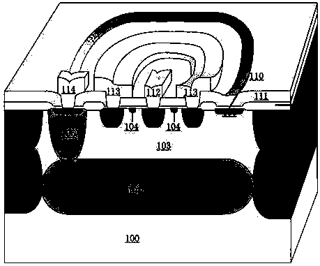
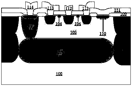
[0059] Such as figure 1 and figure 2 As shown, a lateral high-voltage bipolar junction transistor is characterized in that it includes a P-type substrate 100, an N-type buried layer 101, a P-type buried layer 102, an N-type epitaxial layer 103, and an N-type heavily doped ring region 104. , P-type isolation penetration region 105, N-type penetration region 106, P-type annular body region 107, N-type heavily doped region 108, field oxygen layer 109, pre-oxidation layer 110, TEOS metal pre-dielectric layer 111, emission region metal 112 , collector metal 113 and base metal 114 .

[0060] The N-type buried layer 101 is located at the center of the upper surface of the P-type substrate 100 .

[0061] The P-type buried layer 102 is located at both ends of the upper surface of the P-type substrate 100 .

[0062] The N-type epitaxial layer 103 is located on the N-type buried layer 101 , and the N-type epitaxial layer 103 is in contact with the P-type substrate 100 , the N-type bu...

Embodiment 2

[0075] Such as Figure 3 ~ Figure 11 As shown, a method for manufacturing a lateral high-voltage bipolar junction transistor is characterized in that it comprises the following steps:

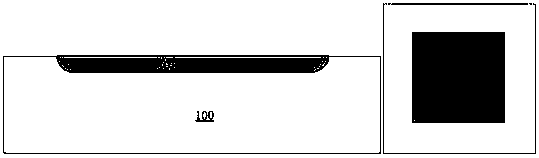
[0076] 1) Select a NTD single chip with less defects, with a thickness of about 500-700 μm and a resistivity of 5-30Ω·cm, marking, cleaning, and drying for later use;

[0077] 2) Growth of a thick oxide layer Temperature 1100~1150℃, time 100min~120min, dry humidification oxidation conditions.

[0078] 3) One photolithography, after photolithography etch to remove glue, grow a thin oxide layer Temperature 1000~1020℃, time 30min~40min, pure dry oxidation conditions.

[0079] The N-type buried layer 101 is implanted in the middle of the wafer substrate, and the ion implantation conditions are: dose 1e15-5e15cm -2 , Energy 40 ~ 80KeV.

[0080] The redistribution conditions are: aerobic conditions 1000 ° C, the thickness of the oxide layer is The re-annealing temperature is pure N2, 1100-11...


PUM


Abstract

The invention discloses a lateral high-voltage bipolar junction transistor and a manufacturing method thereof; comprising a P-type substrate, an N-type buried layer, a P-type buried layer, an N-type epitaxial layer, a P-type isolation penetration region, and an N-type penetration region , P-type body region, N-type heavily doped region, N-type heavily doped ring region, pre-oxidation layer, field oxygen layer, TEOS metal front dielectric layer, emitter metal, collector metal and base metal; the present invention is based on conventional On the basis of the transverse bipolar junction collective tube, an N-type annular injection is added between the collector and the emitter, and then by optimizing the layout of the first layer of metal, the metal is fully covered on the collector. beyond twice the junction depth of the collector region. Through simulation and actual tape-out results, it can be concluded that the horizontal high-voltage bipolar junction transistor of the present invention can increase BVcbo by more than 40%, increase BVceo by more than 30%, and increase the leakage capacity by an order of magnitude when other parameters have little influence. The invention provides a lateral high-voltage bipolar junction transistor.

Description

technical field [0001] The invention relates to a semiconductor device and a manufacturing process, in particular to a lateral high-voltage bipolar junction transistor and a manufacturing method thereof. Background technique [0002] In the mid-1940s, due to the increasingly complex electronic device systems such as navigation, communication, and weaponry, the demand for integration and miniaturization of electronic circuits became increasingly urgent. In 1959, Fairchild Semiconductor Corporation of the United States finally gathered the technological achievements of its predecessors The first practical silicon integrated circuit was manufactured by using planar bipolar process integration technology, which created a precedent for the application and vigorous development of integrated circuits. Most widely, with the continuous advancement of integrated circuit technology, despite the huge challenge of CMOS technology, bipolar technology still develops still by virtue of its ...

Claims


Application Information

Patent Timeline
Patent Type & Authority Applications(China)
IPC IPC(8): H01L29/735H01L21/331H01L29/06H01L29/08
CPCH01L29/08H01L29/0607H01L29/0684H01L29/0821H01L29/6625H01L29/735
Inventor 刘建刘青税国华张剑乔易前宁陈文锁
Owner CHONGQING ZHONGKE YUXIN ELECTRONICS
Why Eureka
Try Eureka