Zn-Sb-Bi thin film material used for multi-state phase change memory, and preparation method of thin film material

A phase-change memory and thin-film material technology, applied in the field of information storage phase-change materials, can solve the problems of high power consumption, loss of phase-change ability and high energy due to material stability, achieve large crystalline resistance, and realize multi-bit multi-value storage , the effect of reducing the chemical bond energy

Active Publication Date: 2018-04-20
NINGBO UNIV
View PDF1 Cites 2 Cited by
  • Summary
  • Abstract
  • Description
  • Claims
  • Application Information

AI Technical Summary

Problems solved by technology

However, if the crystallization temperature is too high, the material will lose its phase transition ability due to its good stability, and the energy required to be applied is too high, resulting in excessive power consumption.

Method used


Image

  • Zn-Sb-Bi thin film material used for multi-state phase change memory, and preparation method of thin film material
  • Zn-Sb-Bi thin film material used for multi-state phase change memory, and preparation method of thin film material
  • Zn-Sb-Bi thin film material used for multi-state phase change memory, and preparation method of thin film material

Examples


Embodiment 1

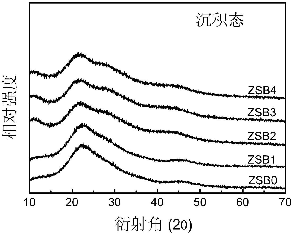
[0023] In the magnetron sputtering coating system, the quartz sheet or silicon oxide sheet is used as the substrate, the metal Bi single target is installed in the magnetron DC sputtering target, and the Zn 2 Sb 3 The alloy target is installed in the magnetron radio frequency sputtering target, and the sputtering chamber of the magnetron sputtering coating system is vacuumed until the vacuum degree of the chamber reaches 5.6×10 -4 Pa, and then pass high-purity argon gas with a volume flow rate of 50ml / min into the sputtering chamber until the air pressure in the sputtering chamber reaches the initiation pressure of 0.3 Pa required for sputtering, and then fix the Zn 2 Sb 3 The sputtering power of the target is 50 W, and the sputtering power of the metal Bi single target is adjusted to 0 W. The double target co-sputters the film at room temperature. After the sputtering thickness reaches 250 nm, the Zn-Sb phase change film in the deposited state is obtained. material whose c...

Embodiment 2

[0026] The same as the first embodiment above, the difference is: during the sputtering process, the sputtering power of the metal Bi single target is controlled to 1 W, and the Zn 2 Sb 3 The sputtering power of the alloy target is 50 W, and the double-target co-sputtering coating is carried out at room temperature. After the sputtering thickness is 250 nm, the as-deposited Zn-Sb-Bi phase-change thin film material is obtained, and its chemical structure is (Zn 2 Sb3 ) 96.8 Bi 3.2 .

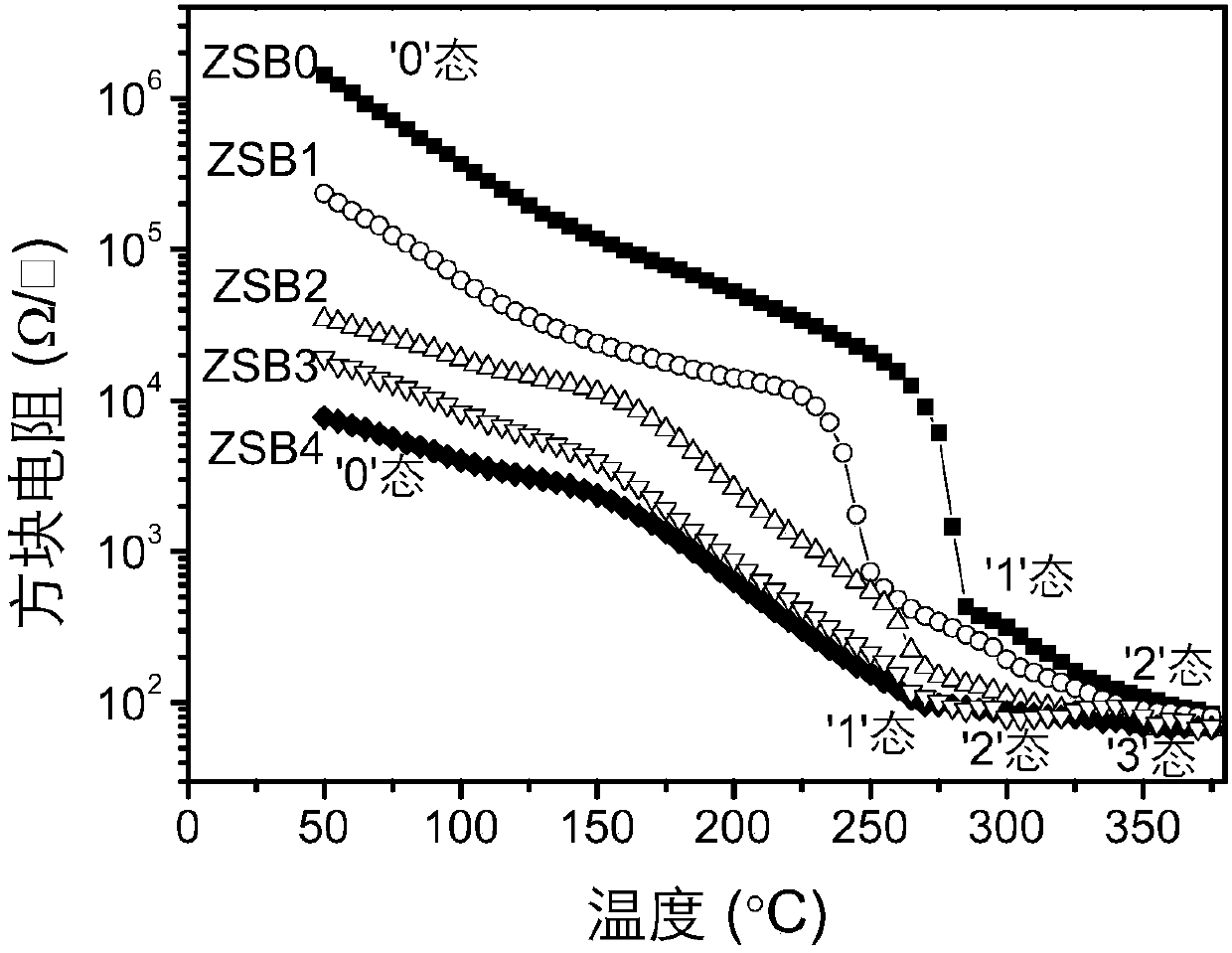
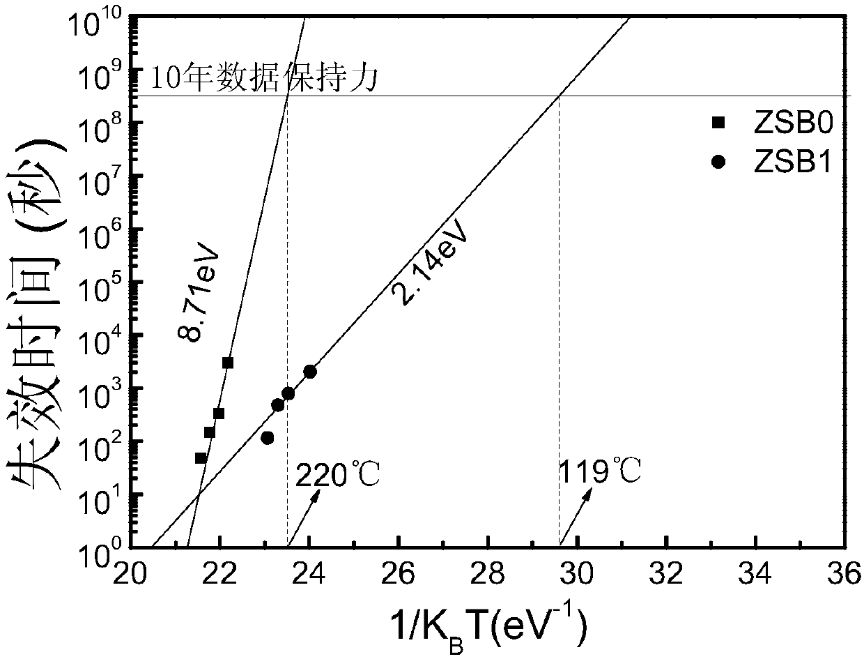
[0027] The prepared thin film material is carried out in-situ resistance and XRD test, find out that the performance index of the thin film prepared in this embodiment is as follows: crystallization temperature T c It is 229 ℃, the phase transition temperature is 320 ℃, the crystallization activation energy is 2.14 eV, the ten-year data retention temperature is 119 ℃, and it has 3 kinds of resistance states.

Embodiment 3

[0029] Same as the first embodiment above, the difference is: during the sputtering process, the sputtering power of the metal Bi single target is controlled to 2 W, and the Zn 2 Sb 3 The sputtering power of the alloy target is 50 W, and the double-target co-sputtering coating is carried out at room temperature. After the sputtering thickness is 250 nm, the deposited Zn-Sb-Bi thin film material is obtained, and its chemical structure is (Zn 2 Sb 3 ) 94.6 Bi 5.4 .

[0030] The prepared thin film material is carried out in-situ resistance and XRD test, find out that the performance index of the thin film prepared in this embodiment is as follows: crystallization temperature T c It is 163 ℃ and has 4 kinds of resistance states.


PUM

PropertyMeasurementUnit
melting pointaaaaaaaaaa
crystallization temperatureaaaaaaaaaa
phase transition temperatureaaaaaaaaaa

Abstract

The invention discloses a Zn-Sb-Bi thin film material used for a multi-state phase change memory, and a preparation method of the thin film material. The thin film material is characterized in that the thin film material is obtained from an elementary metal Bi target and a Zn<2>Sb<3> alloy target in a magnetron sputtering film coating system through dual-target co-sputtering; the thin film material has the chemical structural formula of (Zn<2>Sb<3>)<100-x>Bi<x>, wherein x is greater than or equal to 0 and less than 14, wherein the preferable phase change material Zn<2>Sb<3> and (Zn<2>Sb<3>)<96.8>Bi<3.2> have relatively high crystallization temperature, relatively high crystallization activation energy and relatively high retentivity of data of ten years; and compared with a three-state phase change memory material and the conventional three-state GST phase change material, the thin film material has the advantages of high crystallization temperature and high phase conversion temperature, higher crystalline state resistance and has three resistance states, while the other Zn-Sb-Bi thin film with higher Bi content represents four kinds of resistance states, so that higher multi-bit and multi-valued memory can be realized.

Description

technical field [0001] The invention belongs to the field of phase-change materials for information storage, and in particular relates to a Zn-Sb-Bi film material for multi-state phase-change memory and a preparation method thereof. Background technique [0002] Phase-change memory technology (PCM) is a technology in which the reflectivity / resistivity of phase-change materials can be reversibly changed between amorphous and crystalline states under the action of external light / electric pulses to achieve information storage. It is compatible with the existing integrated circuit semiconductor process (CMOS), and has a long cycle life (greater than 10 12 ), fast read / write speed (20 ns / 10 ns), and little environmental impact, it is widely used in phase change memory. Nowadays, device size reduction is becoming more and more complicated and difficult, and storing multiple data in one device unit is an effective method to increase storage density, so the research on multi-bit st...

Claims


Application Information

Patent Timeline
Patent Type & Authority Applications(China)
IPC IPC(8): H01L45/00
CPCH10N70/231H10N70/881H10N70/026
Inventor 王国祥师道田刘鹏沈祥聂秋华吕业刚
Owner NINGBO UNIV
Why Eureka
Try Eureka