A wafer-level packaging structure and packaging process applied to surface acoustic wave filters

A technology of wafer-level packaging and surface acoustic wave, which is applied in the direction of impedance network and electrical components, can solve the problems of low processing efficiency, low efficiency, and increased bonding force, so as to improve processing efficiency, improve processing efficiency, and reduce heat Mismatch effect

Active Publication Date: 2021-11-16
CETC CHIPS TECH GRP CO LTD
View PDF7 Cites 0 Cited by
  • Summary
  • Abstract
  • Description
  • Claims
  • Application Information

AI Technical Summary

Problems solved by technology

There are two reasons for the large size: First, the diameter of the metal solder ball (gold or tin ball) connected between the chip and the substrate is generally not less than 80um, and a large amount of space needs to be flowed around the solder ball as a margin, which is a lot of waste The chip area is increased; secondly, the bonding force between the organic film used for gas sealing and the substrate is relatively poor, and a large area (200um) around the substrate needs to be occupied to increase the bonding force
[0006] 2. High material cost
If tin balls are used, the volume can be reduced, but the electroplating process will generate a large amount of waste water containing lead, which will pollute the environment and cost a lot of treatment.
If gold balls are used, expensive high-purity gold is required, which is very expensive
3) A special gas-sealed organic film is required to complete the sealing of the device, which is not only costly, but also requires a large substrate area
[0007] 3. Low processing efficiency
Although the above process has improved in terms of device volume and cost, there are still some deficiencies: 1. Due to the use of glue for encapsulation, some bubbles will be generated when the glue is applied, and these bubbles are separated at the beginning, but as time passes Due to the passage of time and the influence of the environment, the bubbles may communicate and eventually communicate with the atmosphere, resulting in a decrease in airtightness; 2. Although the use of monocrystalline silicon wafers as packaging substrates has cost advantages, due to the fixed thermal expansion coefficient of silicon wafers, When bonding with chip substrates of different materials, cracking of the device is prone to occur due to the thermal mismatch between the two; 3. Due to the glue package, the entire filter wafer cannot be bonded to the packaging wafer. Because it is difficult to control the strength of each place just right, it may lead to good bonding effect in some places and poor bonding effect in some places. Therefore, it is necessary to cut the SAW filter wafer into single chips, and bond the cut chips Placed on the silicon wafer substrate where there is glue, so that the chip and the silicon wafer substrate are bonded together, resulting in low efficiency

Method used


Image

  • A wafer-level packaging structure and packaging process applied to surface acoustic wave filters

Examples


Embodiment Construction

[0027] The present invention will be described in detail below in conjunction with the accompanying drawings and specific embodiments.

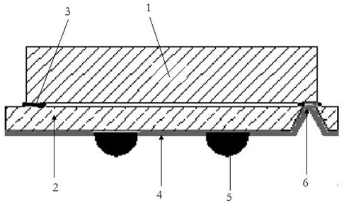
[0028] see figure 1 , it can be seen from the figure that the present invention is applied to the wafer-level packaging structure of the surface acoustic wave filter, including the filter chip substrate 1 (the commonly used material is lithium tantalate) and the packaging wafer 2, in the filter chip A circle of gold film 3 is plated on the periphery of the working surface of the substrate 1, and a circle of gold film 3 is also plated on the package wafer 2 corresponding to the gold film of each chip substrate, and the filter chip substrate 1 and the package wafer 2 pass through gold-gold bonding. An external circuit wiring structure 4 and metal solder balls 5 (usually gold balls or tin balls) for electrical connection with the PCB board are provided on the side of the packaging wafer 2 facing away from the working surface of the chip. The t...


PUM


Abstract

The invention discloses a wafer-level packaging structure and packaging technology applied to surface acoustic wave filters, including a filter chip substrate and a packaging wafer, and a circle of gold film is coated on the periphery of the working surface of the filter chip substrate. The position corresponding to the gold film on each chip substrate on the packaging wafer is also coated with a circle of gold film, and the filter chip and the packaging wafer are combined by gold-gold bonding; There are external circuit wiring structures and metal solder balls for electrical connection with the PCB board, and via holes are provided on the packaging wafer to electrically connect the circuit on the chip working surface to the metal solder balls through the via holes and the external circuit wiring structure in turn. The packaging wafer is made of glass material, and the glass material has the same or close thermal expansion coefficient as that of the chip substrate material. The packaging of the invention is more reliable, the efficiency is improved, and the thermal mismatch of devices can be easily eliminated.

Description

technical field [0001] The invention relates to a surface acoustic wave filter, in particular to a wafer-level packaging structure and a packaging process applied to a surface acoustic wave filter, and belongs to the technical field of surface acoustic wave filter packaging. Background technique [0002] Do not directly contact the working surface of the surface acoustic wave filter chip with air or moisture, which will cause corrosion or oxidation on the working surface and affect the performance of the device. Therefore, in actual processing, the working surface of the chip needs to be packaged to protect it. After packaging Then connect with the PCB board. [0003] Existing SAW filters are mainly packaged by flip-chip soldering (CSP) technology. The basic principle of CSP packaging is very simple. First, metal solder balls (gold or tin) are grown on the wafer forming the chip by ultrasonic welding or reflow soldering process, then cut into individual chips, and then flip...

Claims


Application Information

Patent Timeline
Patent Type & Authority Patents(China)
IPC IPC(8): H03H9/02H03H9/64
CPCH03H9/02543H03H9/02622H03H9/64
Inventor 金中何西良杜雪松
Owner CETC CHIPS TECH GRP CO LTD
Why Eureka
Try Eureka