Method for preparing crystalline-state nano structure based on femtosecond laser-induced amorphous GemSbnTek thin film

A nanostructure and femtosecond laser technology, applied in the field of femtosecond laser applications, can solve the problems of high precision requirements of processing platforms, restricting applications, limiting processing efficiency, etc., and achieve the effect of improving processing accuracy and processing efficiency

Active Publication Date: 2018-05-11
BEIJING UNIV OF TECH
View PDF8 Cites 24 Cited by
  • Summary
  • Abstract
  • Description
  • Claims
  • Application Information

AI Technical Summary

Problems solved by technology

However, this processing method has high requirements on the accuracy of the processing platform for small laser direct writing wire cutting, and the excessive number of laser pulses limits the processing efficiency and restricts its wide application.

Method used


Image

  • Method for preparing crystalline-state nano structure based on femtosecond laser-induced amorphous GemSbnTek thin film
  • Method for preparing crystalline-state nano structure based on femtosecond laser-induced amorphous GemSbnTek thin film

Examples


Embodiment

[0033] Crystalline Ge 2 Sb 2 Te 5 Take the nanoparticle array as an example, using the single pulse femtosecond laser processing method of the present invention, the femtosecond laser pulse used is linearly polarized, and the specific processing steps are as follows:

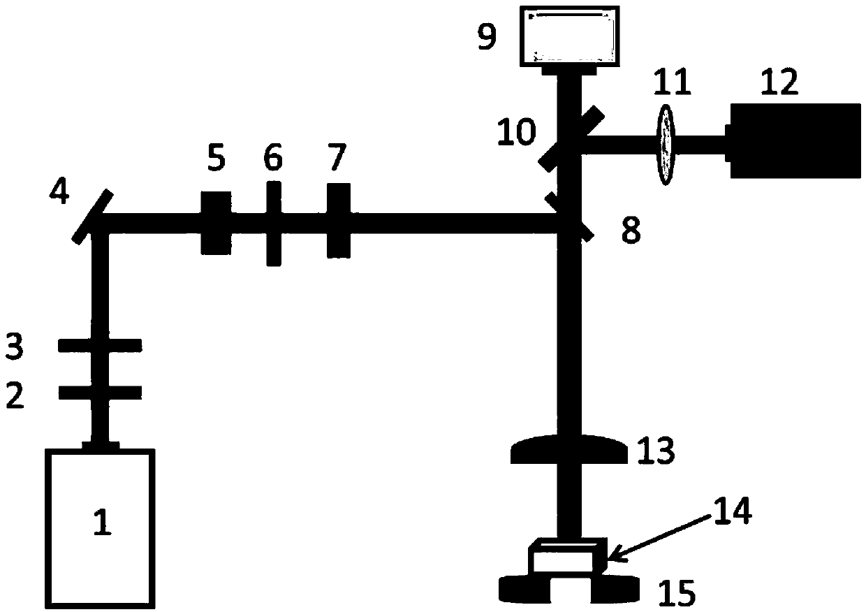
[0034] Adjust the optical path to ensure that the laser incident direction is perpendicular to the surface of the processed sample;

[0035] (1) Sample preparation: In this embodiment, a single crystal silicon sample of 10mm×10mm×1mm is plated with 50nmGe by magnetron sputtering. 2 Sb 2 Te 5 Film (the adjustable range of film thickness is 20nm~70nm), Ge m Sb n Te k The m, n, and k values ​​of can be controlled to different values ​​by magnetron sputtering targets.

[0036] (2) Adjust the energy: use the half-wave plate 2-polarizer 3 combination and the continuous attenuator 5 to adjust the laser energy to be greater than the single pulse ablation threshold of the processed sample material surface, and the laser energy c...

Embodiment 2

[0041] Crystalline Ge 2 Sb 2 Te 5 Take the nanoparticle array as an example, the single pulse femtosecond laser processing method of the present invention is adopted, and the femtosecond laser pulses used are circularly polarized. The specific processing steps are as follows:

[0042] The other steps are the same as in embodiment 1, but the difference is: before step (2) energy adjustment is carried out, a quarter wave plate 6 is added to the optical path, and the quarter wave plate 6 is adjusted so that the optical axis direction of the wave plate is aligned with The original laser polarization direction included an angle of 45° to obtain a circularly polarized 800nm ​​femtosecond laser pulse. Processing is performed under the condition of circularly polarized femtosecond laser pulses.

Embodiment 1、2

[0043] Comparison results of Examples 1 and 2:

[0044] Because the structure formed on the surface produces a plasma-like effect under the action of the laser polarity, the surface plasma field generated by the excitation is distributed along the radial direction, and the material converges toward the center under a relatively uniform stress. Therefore, the circle is adopted in the second embodiment. Crystalline Ge processed by polarized femtosecond laser pulse 2 Sb 2 Te 5 The nanoparticle structure is not easy to bend, and the shape is better.


PUM

PropertyMeasurementUnit
thicknessaaaaaaaaaa

Abstract

The invention discloses a method for preparing a crystalline-state nano structure based on a femtosecond laser-induced amorphous GemSbnTek thin film, and belongs to the technical field of femtosecondlaser application. The size of a single incident femtosecond laser pulse focused light spot is controlled within a certain energy range, so that control over processing and the size of the GemSbnTek crystalline-state nano particle is realized, when the focused light spot is relatively large, the nano particle with a relatively large diameter can be obtained, and when the size of the focused lightspot is reduced, the diameter of the nano particle can be reduced. The laser frequency and the movement speed of a translation table are integrally controlled so that large-area efficient preparationof the high-consistency and uniform crystalline-state nano particle can be further realized. According to the method, compared with an existing nano structure processing method, the processing precision and processing efficiency of the nano structure are effectively improved, controllable preparation of the single nano structure and the composite nano structure is realized, meanwhile, the change of the crystalline nature of the super-fast phase change material GemSbnTek nano structure is realized, and the method has critical application value in the aspects such as information storage, metamaterial, nanometer antennas and light control.

Description

Technical field [0001] The present invention relates to femtosecond laser induced amorphous Ge m Sb n Te k A method for preparing a crystalline nanostructure by a thin film belongs to the technical field of femtosecond laser application. Background technique [0002] Compared with the traditional long pulse, ultrafast laser and its micro-nano manufacturing have unique properties of ultra-fast, super-strong, three-dimensional and ultra-precision, and are one of the frontiers of contemporary micro-nano manufacturing methods. As a kind of ultrafast laser, the three characteristics of femtosecond laser make femtosecond laser micro-nano processing have unique advantages. Micro-nano materials have a variety of excellent properties and have far-reaching application prospects in the fields of optics, optoelectronics, photonics, plasma, photobiosensing, micro-nano fluids, microfluidic optics, and biomedicine. In these fields, surface micro-nano technology as an effective method can chang...

Claims


Application Information

Patent Timeline
Patent Type & Authority Applications(China)
IPC IPC(8): B23K26/00B23K26/362B82Y40/00
CPCB23K26/00B23K26/361B82Y40/00
Inventor 韩伟娜刘富荣袁艳萍
Owner BEIJING UNIV OF TECH
Why Eureka
Try Eureka