Field effect transistor based on vertical tunneling, biosensor and preparation methods thereof

A field-effect transistor and tunneling technology, applied in semiconductor/solid-state device manufacturing, semiconductor devices, instruments, etc., can solve the problems of low device structure sensitivity, poor detection accuracy, poor reliability, etc., and achieve strong controllability and low cost. , to ensure the effect of accuracy

Inactive Publication Date: 2018-05-25
SHANGHAI INST OF MICROSYSTEM & INFORMATION TECH CHINESE ACAD OF SCI
View PDF3 Cites 5 Cited by
  • Summary
  • Abstract
  • Description
  • Claims
  • Application Information

AI Technical Summary

Problems solved by technology

[0006] In view of the shortcomings of the prior art described above, the object of the present invention is to provide a field effect transistor, a biosensor and their respective preparation methods, which are used to solve the problems of low device structure sensitivity, high power consumption, poor reliability and detection problems in the prior art. poor accuracy

Method used


Image

  • Field effect transistor based on vertical tunneling, biosensor and preparation methods thereof
  • Field effect transistor based on vertical tunneling, biosensor and preparation methods thereof
  • Field effect transistor based on vertical tunneling, biosensor and preparation methods thereof

Examples


Embodiment 1

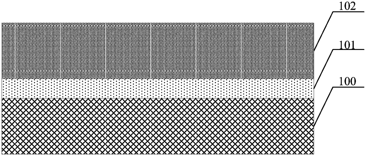
[0073] like figure 1 As shown, the present invention provides a method for preparing a field effect transistor based on vertical tunneling, comprising the following steps:

[0074] 1) providing an SOI substrate, the SOI substrate includes a bottom layer silicon, a buried oxide layer and a top layer silicon;

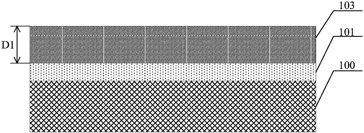
[0075] 2) thinning the top layer silicon to a first thickness, and using a photolithography process to define a silicon nanowire channel pattern and a source region pattern and a drain region pattern connected to both ends of the silicon nanowire channel pattern;

[0076] 3) using an etching process to transfer the silicon nanowire channel pattern, source region pattern and drain region pattern to the top layer silicon, and perform ion implantation of the first conductivity type to the position corresponding to the source region pattern, performing ion implantation of the second conductivity type to a position corresponding to the drain pattern to form a silicon nanowire...

Embodiment 2

[0117] This embodiment provides a method for preparing a biosensor, comprising the following steps:

[0118] 1) using the preparation method described in any one of the embodiments to prepare a field effect transistor based on vertical tunneling;

[0119] 2) using reagents to modify the surface of the silicon nanowire channel 109 of the field effect transistor to form a layer of active thin film ending with active groups;

[0120] 3) forming a capture probe on the surface of the active film, wherein the capture probe is combined with an active group on the active film through chemical bonds, so that the capture probe is modified in the silicon nanowire groove surface of the road.

[0121] Specifically, the present invention also provides a biosensor based on a vertical tunneling field effect transistor, wherein, in this embodiment, the surface of the nanowire channel unit is modified by using a reagent to form a layer by self-assembly Reactive films terminated by reactive gr...


PUM

PropertyMeasurementUnit
widthaaaaaaaaaa
thicknessaaaaaaaaaa
thicknessaaaaaaaaaa

Abstract

The invention provides a field effect transistor based on vertical tunneling, a biosensor and preparation methods thereof. The preparation method of the field effect transistor comprises the followingsteps: providing an SOI substrate; thinning top silicon, and defining a silicon nanowire channel pattern and a source region pattern and a drain region pattern connected at the two ends; transferringthe patterns above to the top silicon, and carrying out ion implantation to form a silicon nanowire channel, a source region and a drain region; thinning the source region, and forming a dielectric layer on a part of source region surface and nanowire channel surface; and preparing a source electrode on the surface of the source region, preparing a drain electrode on the surface of the drain region, and preparing a gate electrode on bottom silicon or a buried oxide layer. Through the scheme above, the transistor based on vertical tunneling comprises point tunneling and line tunneling, has lower sub-threshold slope, can be used for high-sensitivity biochemical molecular detection, has bipolar characteristics, can carry out comparison on bidirectional detection results and ensures detectionaccuracy; and through the high-K dielectric layer material, detection stability is enhanced and response capability for biomolecule is improved.

Description

technical field [0001] The invention belongs to the technical field of semiconductor device manufacturing, and in particular relates to a field effect transistor, a biosensor and their respective preparation methods. Background technique [0002] Semiconductor biosensors are sensors composed of biomolecular recognition devices (biosensitive films) and semiconductor devices. Biosensors based on semiconductor field effect transistors (FET) are simple in structure, low in cost, and convenient for mass production; good mechanical properties , good seismic performance, long life; low output impedance, easy to match with subsequent circuits; multiple sensors can be integrated on the same chip, which can achieve multi-function, multi-parameter detection and other advantages, semiconductor field effect transistor biosensors are considered to be the most One of the devices with application potential. [0003] Among them, the semiconductor field effect transistor sensor based on sili...

Claims


Application Information

Patent Timeline
Patent Type & Authority Applications(China)
IPC IPC(8): H01L29/739H01L21/331H01L29/10G01N27/00
CPCG01N27/00H01L29/1025H01L29/66356H01L29/7391
Inventor 高安然赵兰天赵清太李铁王跃林
Owner SHANGHAI INST OF MICROSYSTEM & INFORMATION TECH CHINESE ACAD OF SCI
Why Eureka
Try Eureka