Light-emitting diode epitaxial wafer and preparation method thereof

A technology of light-emitting diodes and epitaxial wafers, applied in electrical components, circuits, semiconductor devices, etc., can solve the problems of shock damage to the crystal structure of the buffer layer, and achieve the effects of improving reliability, prolonging service life, and avoiding shocks

Active Publication Date: 2018-05-25
HC SEMITEK ZHEJIANG CO LTD
View PDF7 Cites 4 Cited by
  • Summary
  • Abstract
  • Description
  • Claims
  • Application Information

AI Technical Summary

Problems solved by technology

[0008] In order to solve the problem that the crystal structure of the buffer layer is damaged by the impact caused by electron diffusion to the buffer layer in the prior art, an embodiment of the present invention provides a light-emitting diode epitaxial wafer and a preparation method thereof

Method used


Image

  • Light-emitting diode epitaxial wafer and preparation method thereof
  • Light-emitting diode epitaxial wafer and preparation method thereof
  • Light-emitting diode epitaxial wafer and preparation method thereof

Examples


Embodiment 1

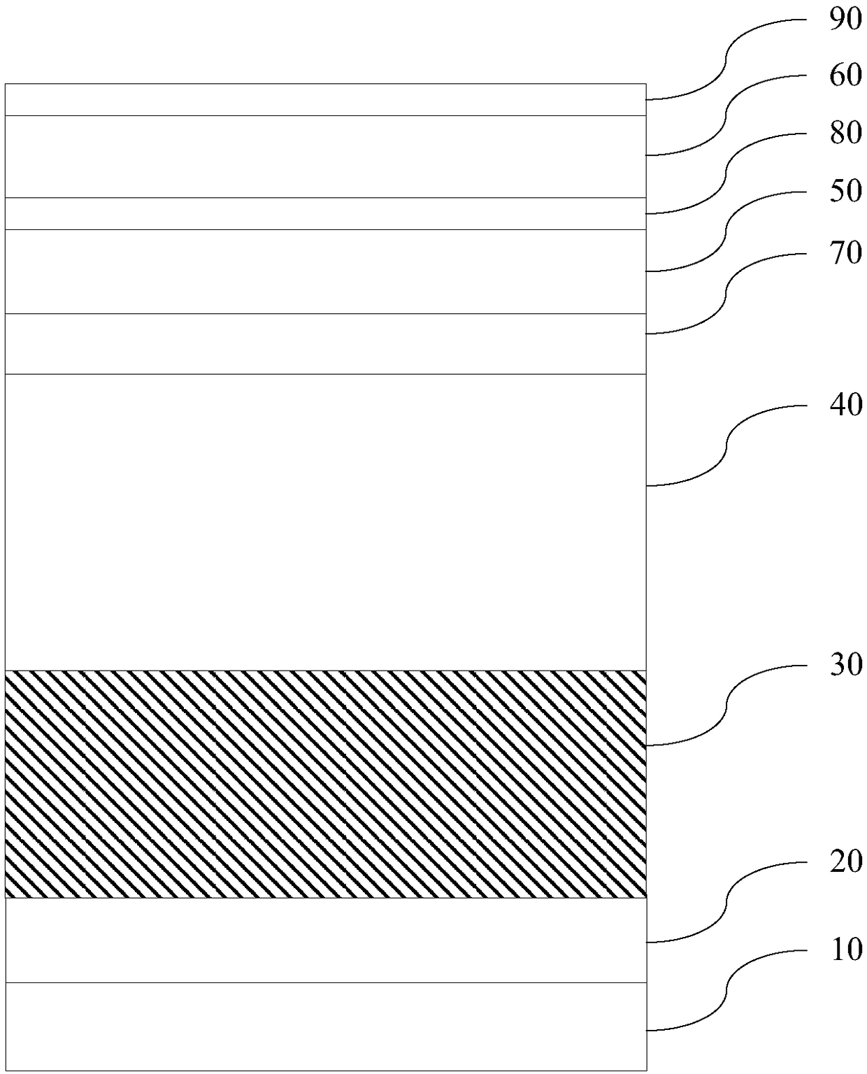
[0033] An embodiment of the present invention provides a light emitting diode epitaxial wafer, figure 1 For the structural schematic diagram of the light-emitting diode epitaxial wafer provided in this embodiment, see figure 1 , the light-emitting diode epitaxial wafer includes a substrate 10 and a low-temperature buffer layer 20, a high-temperature buffer layer 30, an N-type gallium nitride layer 40, a multi-quantum well layer 50 and a P-type gallium nitride layer 60 stacked on the substrate 10 in sequence. .

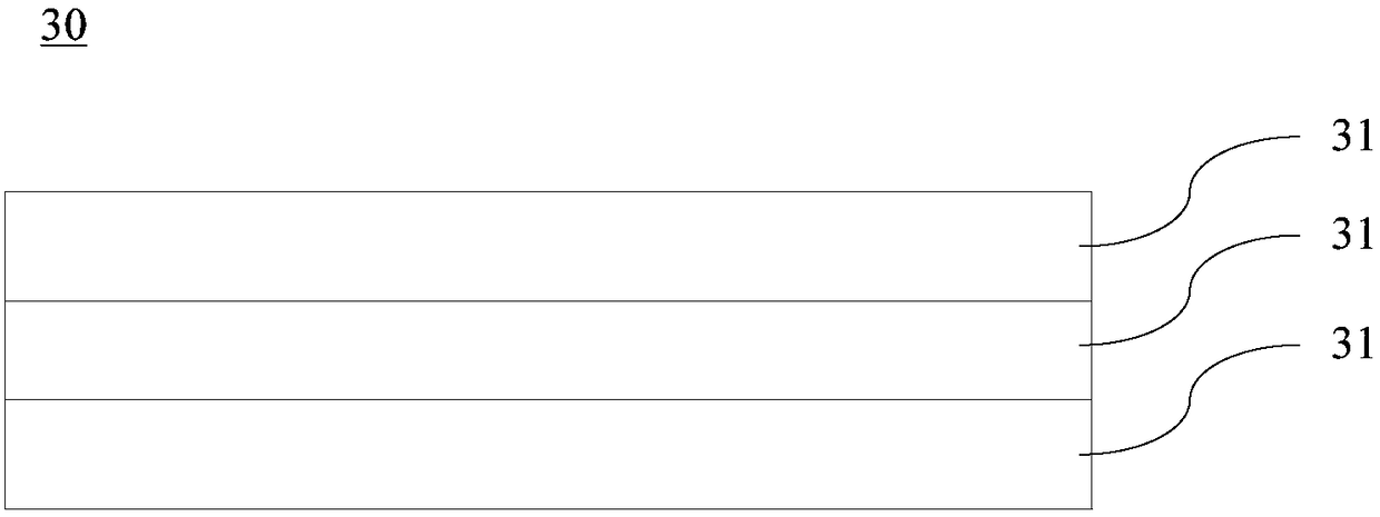
[0034] figure 2 For the structural representation of the high-temperature buffer layer provided in this embodiment, see figure 2 , in this embodiment, the high-temperature buffer layer 30 includes (2*n+1) sub-layers 31 stacked in sequence, where n is a positive integer ( figure 2 Take n=1 as an example). Each sub-layer 31 is a P-type doped gallium nitride layer, and the doping concentration of the P-type dopant in (2*n+1) sub-layers 31 decreases layer by layer a...

Embodiment 2

[0070] The embodiment of the present invention provides a method for preparing a light emitting diode epitaxial wafer, which is suitable for preparing the light emitting diode epitaxial wafer provided in the first embodiment. Figure 4 For the flow chart of the preparation method provided in this embodiment, see Figure 4 , the preparation method comprises:

[0071] Step 201: Provide a substrate.

[0072] Step 202: growing a low-temperature buffer layer, a high-temperature buffer layer, an N-type GaN layer, a multi-quantum well layer, and a P-type GaN layer sequentially on the substrate.

[0073]In this embodiment, the high-temperature buffer layer includes (2*n+1) sublayers stacked in sequence, n is a positive integer, each sublayer is a P-type doped gallium nitride layer, and (2*n+1) sublayers The doping concentration of the P-type dopant in the layer decreases layer by layer along the stacking direction of the high-temperature buffer layer, and the doping concentration of...

Embodiment 3

[0100] The embodiment of the present invention provides a method for preparing a light-emitting diode epitaxial wafer, which is a specific implementation of the method provided in the second embodiment. Figure 5 For the flow chart of the preparation method provided in this embodiment, see Figure 5 , the preparation method comprises:

[0101] Step 301: Control the processing temperature to 350° C. and the sputtering pressure to 25 mTorr, and sputter an aluminum target under a nitrogen atmosphere to form an aluminum nitride layer with a thickness of 150 nm in a low-temperature buffer layer on the PSS.

[0102] Step 302: Control the processing temperature to 700° C. and the sputtering pressure to 25 mTorr, and sputter the aluminum target under nitrogen atmosphere to form a high-temperature aluminum nitride layer with a thickness of 70 nm on the aluminum nitride layer in the low-temperature buffer layer.

[0103] Step 303: Treat the aluminum nitride layer and the high-temperatu...


PUM

PropertyMeasurementUnit
temperatureaaaaaaaaaa
thicknessaaaaaaaaaa
thicknessaaaaaaaaaa

Abstract

The invention discloses a light-emitting diode epitaxial wafer and a preparation method thereof, and belongs to the technical field of a semiconductor. The light-emitting diode epitaxial wafer comprises a substrate, a low-temperature buffer layer, a high-temperature buffer layer, an N-type gallium nitride layer, a multi-quantum well layer and a P-type gallium nitride layer, wherein the low-temperature buffer layer, the high-temperature buffer layer, the N-type gallium nitride layer, the multi-quantum well layer and the P-type gallium nitride layer are stacked up on the substrate in sequence. The high-temperature buffer layer comprises (2*n+1) sublayers stacked up in sequence, n being a positive integer. Each sublayer is a P-type doped gallium nitride layer; doping concentration of P-type dopants in the (2*n+1) sublayers is reduced layer by layer in the stack direction of the high-temperature buffer layer; the doping concentration of the P-type dopants in two adjacent sublayers differsby one order of magnitude; and the order of magnitude of doping concentration of the P-type dopants in the (n+1) th stacked sublayer is same with the order of magnitude of electron concentration in the undoped gallium nitride layer. The light-emitting diode epitaxial wafer can carry out effective blocking on diffused electrons in the N-type gallium nitride layer, thereby improving reliability of the LED.

Description

technical field [0001] The invention relates to the technical field of semiconductors, in particular to a light-emitting diode epitaxial wafer and a preparation method thereof. Background technique [0002] Light Emitting Diode (English: Light Emitting Diode, referred to as: LED) is a new generation of solid-state lighting source with high efficiency, environmental protection and green, which has the advantages of low voltage, low power consumption, small size, light weight, long life and high reliability. quickly and widely used. The core part of the LED is the chip, and the chip includes an epitaxial wafer and electrodes arranged on the epitaxial wafer. [0003] At present, the material of the epitaxial wafer is mainly gallium nitride, which is a semiconductor material with a wide bandgap (the bandgap width is about 3.4eV), which can generate blue light, and the produced blue light can be passed through the yellow phosphor to obtain white light. Since the GaN-based LED e...

Claims


Application Information

Patent Timeline
Patent Type & Authority Applications(China)
IPC IPC(8): H01L33/12H01L33/14H01L33/00
Inventor 兰叶顾小云王江波
Owner HC SEMITEK ZHEJIANG CO LTD
Why Eureka
Try Eureka