Preparation method of dimension-controllable CsPbX3 perovskite nanometer crystals

A perovskite and nanocrystal technology, applied in the synthesis of high-quality CsPbX3 perovskite nanocrystals, can solve the problems of unstable particles, less controllable reactions, narrow emission half-peak widths, etc. Control, product size easy to adjust, simple operation effect

Inactive Publication Date: 2018-06-01
JILIN UNIV
View PDF4 Cites 15 Cited by
  • Summary
  • Abstract
  • Description
  • Claims
  • Application Information

AI Technical Summary

Problems solved by technology

However, the perovskite nanocrystals prepared by this method are hot injected at high temperature and there are a large number of unreacted inorganic salts and organic ligands, which makes the whole reaction uncontrollable. Therefore, the synthesized by this method Halogen-lead-cesium perovskite nanocrystals have a certain size distribution
When the size of the nanocrystal is not very uniform, it will show a broadening of its absorption and emission spectrum, and its absorption and emission half-peak width will increase, that is to say, the emitted fluorescence is not very pure. , which will limit the application of pure inorganic perovskite nanocrystals in display and imaging
However, the xie group can obtain a series of single-size CsPbX by adjusting the ratio of oleylamine through room temperature reaction. 3 Perovskite nanocrystals, although this kind of perovskite nanocrystals have extremely narrow emission half-peak width and fluorescence purity, but because they are synthesized at room temperature, the particle size is very small (no more than 4nm), so the particles are not very Stable, prone to self-decomposition
[0004] In summary, the existing inorganic perovskite nanocrystals have certain limitations, there are unresolved problems and defects, and the technology needs to be innovated and improved.

Method used


Image

  • Preparation method of dimension-controllable CsPbX3 perovskite nanometer crystals
  • Preparation method of dimension-controllable CsPbX3 perovskite nanometer crystals
  • Preparation method of dimension-controllable CsPbX3 perovskite nanometer crystals

Examples


Embodiment 1

[0026] First, a cesium oleate solution is prepared. Take 2mmol (0.648g) of cesium carbonate powder, 10mmol (3.35mL) of OA (oleic acid) and 6.65mL of ODE (octadecene) and mix, heat to 150°C under nitrogen protection to dissolve cesium carbonate, cool to 100 ℃, prepared into 0.2M cesium oleate solution, which was light yellow transparent solution.

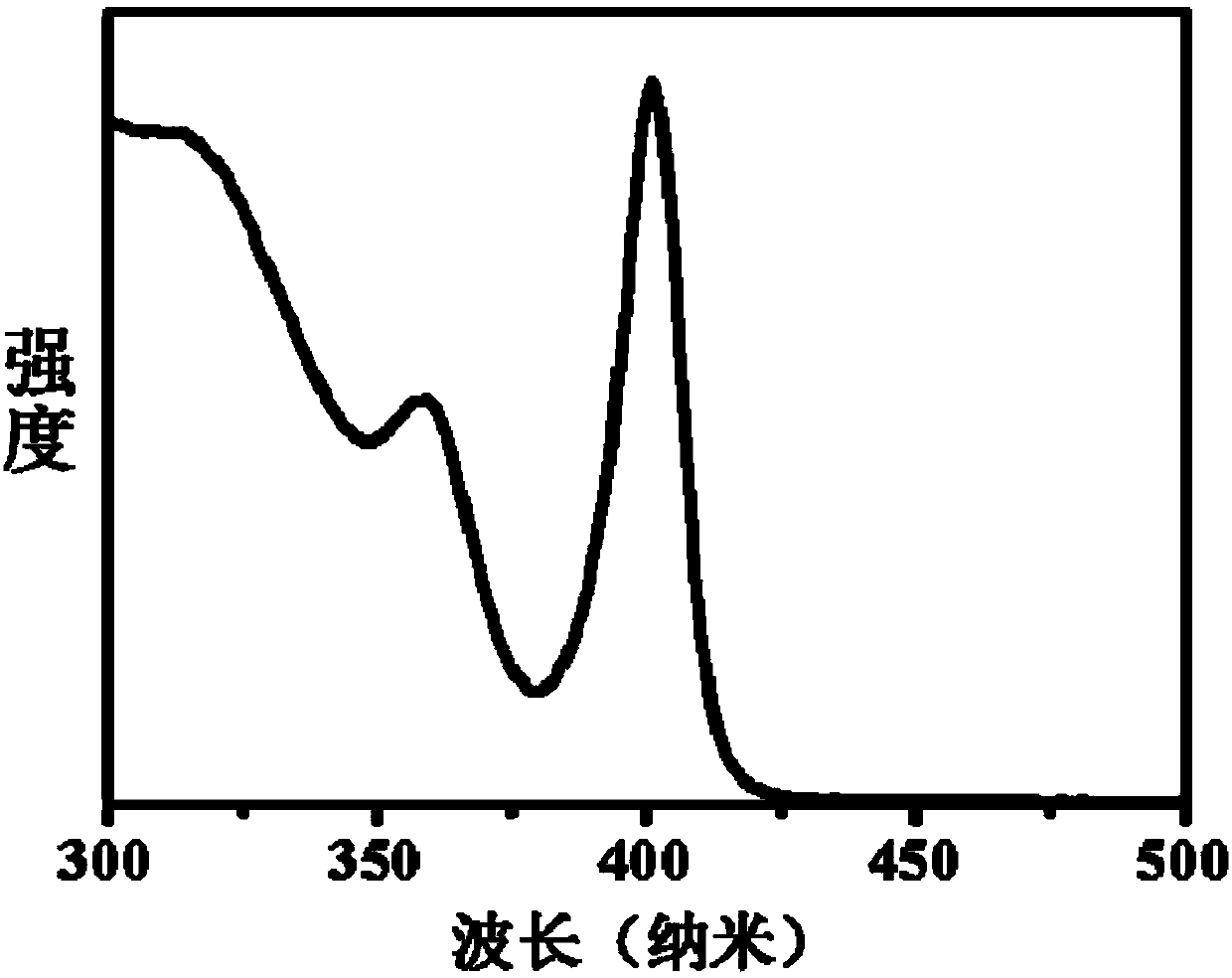
[0027] Then take 0.2mmol of lead bromide solid powder, 0.6mL of oleylamine, 0.6mL of oleic acid and 2.8mL of octadecene into the three-necked flask, vacuumize at 50°C for 30 minutes, fill with nitrogen protection, and then heat up to 150°C , after the lead bromide is dissolved, lower it to room temperature 25°C, and then inject 0.2mL of 0.2M cesium oleate octadecene solution, and react to obtain CsPbBr with an absorption peak at 402nm 3 Perovskite nanocrystalline seeds. Its absorption spectrum is shown in figure 1 .

Embodiment 2

[0029] The 0.04mmol of CsPbBr prepared in Example 1 3 The perovskite nanocrystal seeds were centrifuged, precipitated and separated, and then dispersed into 1 mL of n-hexane.

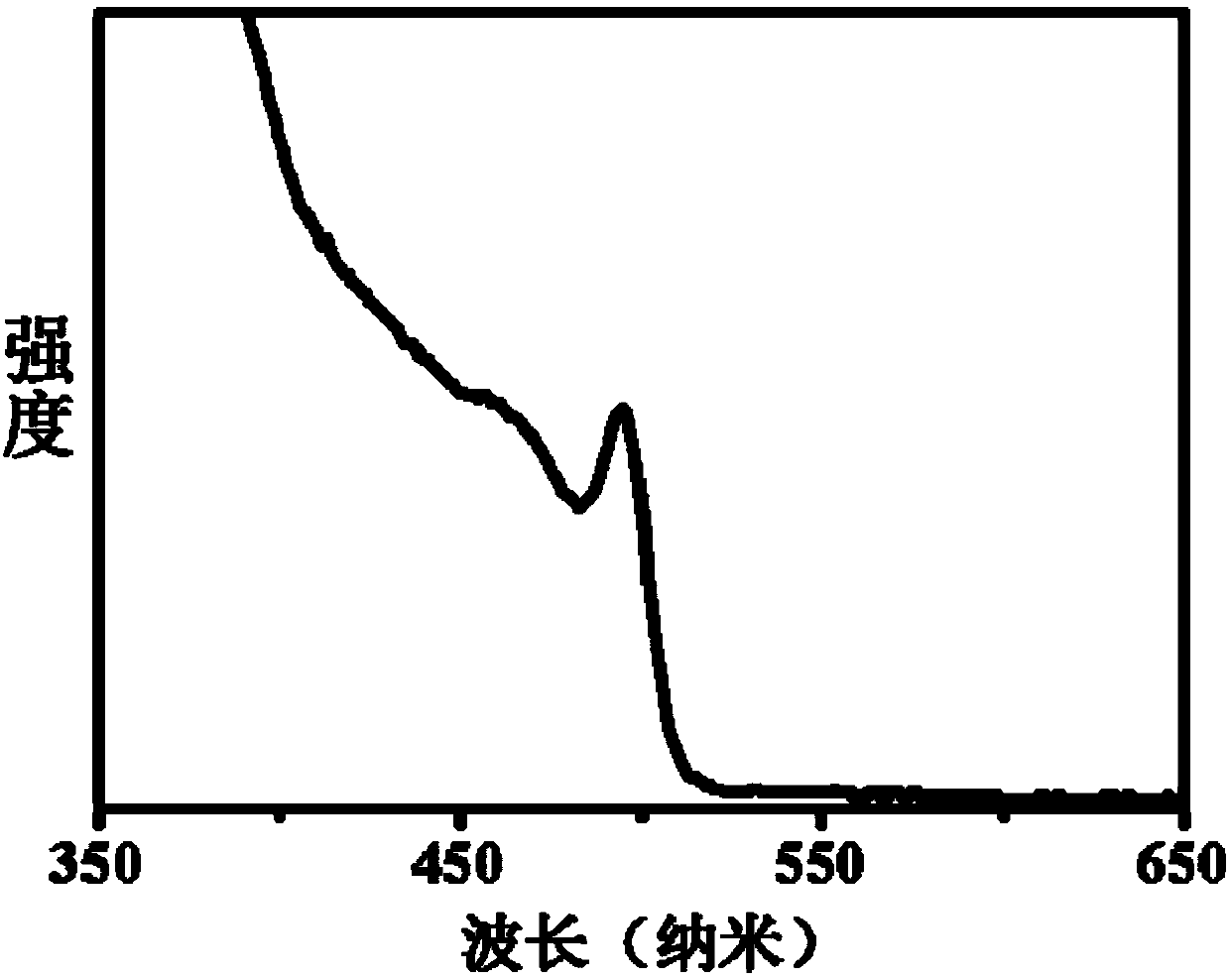
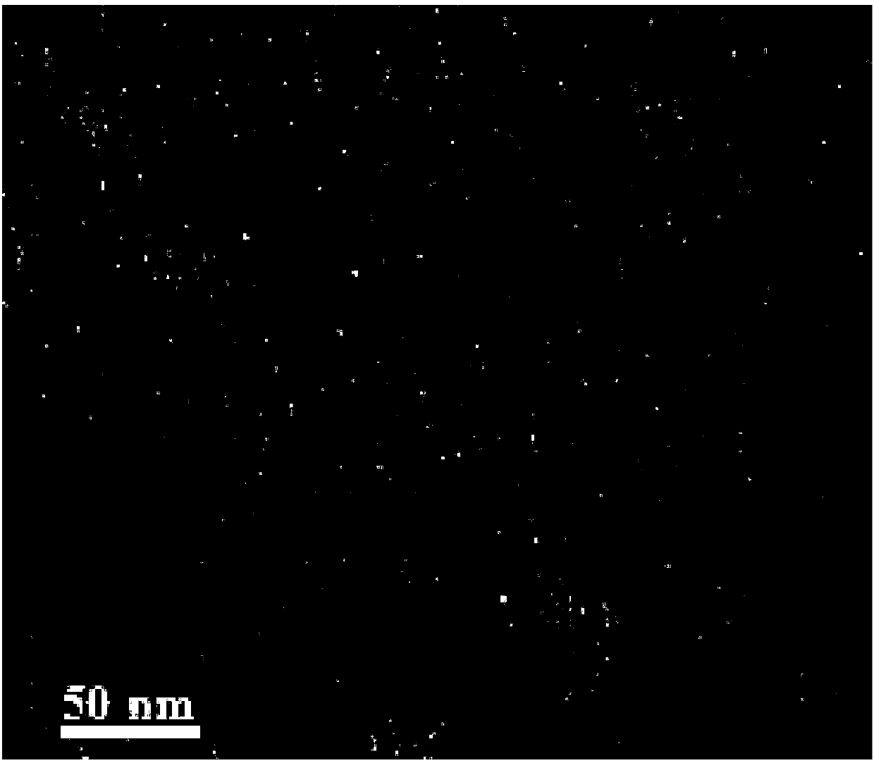
[0030] Add 4 mL of octadecene to a three-necked flask, vacuumize at 100°C for 30 minutes, fill with nitrogen, keep at 100°C, and then inject 1 mL of CsPbBr 3The n-hexane solution of perovskite nanocrystal seeds reacts to obtain CsPbBr with an absorption peak at 495nm 3 Perovskite nanocrystals with a particle size of 6nm. Its absorption spectrum is shown in figure 2 , see its electron micrograph image 3 .

Embodiment 3

[0032] The 0.04mmol of CsPbBr prepared in Example 1 3 The perovskite nanocrystal seeds were centrifuged, precipitated and separated, and then dispersed into 1 mL of n-hexane.

[0033] Take 4mL of octadecene and add it to a three-necked bottle, vacuumize it at 100°C for 30 minutes, fill it with nitrogen for protection, then raise the temperature to 140°C, and then inject the above 1mL CsPbBr 3 The n-hexane solution of perovskite nanocrystal seeds reacts to obtain CsPbBr with an absorption peak at 507nm 3 Perovskite nanocrystals with a particle size of 12nm. Its absorption spectrum is shown in Figure 4 , see its electron micrograph Figure 5 .


PUM

PropertyMeasurementUnit
sizeaaaaaaaaaa

Abstract

The present invention relates to a preparation method of dimension-controllable CsPbX3 perovskite nanometer crystals, and belongs to the technical field of preparation of a semiconductor nanomaterial.The method comprises: firstly, adding a cesium carboxylate solution to a lead bromide solution in N2 protection for a reaction, thereby obtaining CsPbBr3 perovskite nanometer crystal seeds; then, dispersing CsPbBr3 perovskite nanometer crystal seeds in hexane, injecting the obtained product to octadecene at different temperature to obtain CsPbBr3 perovskite nanometer crystals with different sizes; and finally, dispersing CsPbBr3 perovskite nanometer crystals in hexane, and gradually adding a lead chloride solution or a lead iodide solution drop by drop for a reaction to obtain other CsPbX3 (X=Cl, Ir) perovskite nanometer crystals. The method is simple to operate, the size of products is easy to adjust, and the components are controllable.

Description

technical field [0001] The invention belongs to the technical field of semiconductor nanomaterial preparation, in particular to a high-quality CsPbX with controllable size 3 (X=Cl, Br, I) Synthetic method of perovskite nanocrystals. Background technique [0002] After the semiconductor material is gradually reduced from the bulk phase to a certain critical size (1-20 nanometers), the volatility of the carriers becomes significant, and the movement will be limited, resulting in an increase in kinetic energy. The corresponding electronic structure is continuous from the bulk phase to The energy level structure becomes a quasi-split discontinuity, a phenomenon known as the quantum size effect. The more common semiconductor nanoparticles, that is, quantum dots, mainly include II-VI, III-V and IV-VI groups. These types of quantum dots are well obeyed by the quantum size effect, and their properties change regularly with the size, for example, the absorption and emission wavelen...

Claims


Application Information

Patent Timeline
Patent Type & Authority Applications(China)
IPC IPC(8): C01G21/00B82Y40/00
CPCB82Y40/00C01G21/00C01P2002/34C01P2004/01C01P2004/64
Inventor 张颖杨悦解仁国汪大洋杨文胜
Owner JILIN UNIV
Why Eureka
Try Eureka