

TSV switching plate for system in package
A system-in-package, adapter board technology, applied in the direction of semiconductor/solid-state device components, diodes, semiconductor devices, etc., can solve problems such as inability to meet, achieve high heat dissipation capacity, enhanced antistatic capacity, small leakage current and parasitic The effect of capacitors
- Summary
- Abstract
- Description
- Claims
- Application Information
AI Technical Summary
Problems solved by technology
Method used
Image

Examples
Embodiment 1
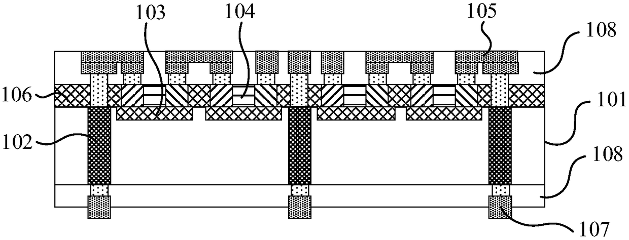
[0030] See figure 1 , figure 1 It is a schematic structural diagram of a TSV interposer board for system-in-package provided by an embodiment of the present invention, including:
[0031] Si substrate 101;
[0032] At least two TSV regions 102 are provided in the Si substrate 101;
[0033] At least two isolation regions 103 are arranged in the Si substrate 101 and located between every two TSV regions 102;
[0034] The diode 104 is arranged on the isolation region 103;
[0035] The interconnection line 105 connects the first end surface of the TSV area 102 and the diode 104 in series.
[0036] Specifically, it also includes a passivation layer 106, which is disposed on the Si substrate 101 and used to isolate the TSV region 102 from the diode 104 and the diode 104.
[0037] Preferably, the material in the TSV region 102 is polysilicon, and the doping concentration of the polysilicon is 2×10 21 cm -3 , The doped impurity is phosphorus.
[0038] Preferably, the TSV region 102 penetrates the ...
Embodiment 2
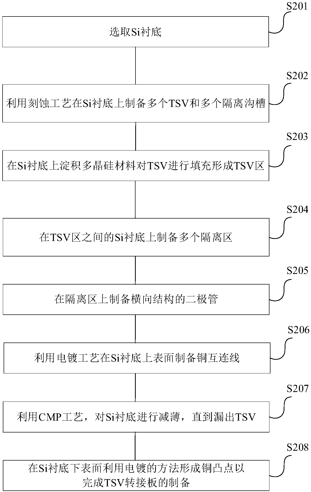
[0047] Please refer to figure 2 , figure 2 This is a flow chart of a method for preparing a TSV interposer board for system-in-package according to an embodiment of the present invention. Based on the above embodiments, the method for preparing the TSV interposer board of the present invention is described in detail in this embodiment as follows . Specifically, it includes the following steps:
[0048] S201. Select a Si substrate;
[0049] S202, preparing multiple TSVs on the Si substrate by using an etching process;
[0050] S203, depositing polysilicon material on the Si substrate to fill the TSV to form a TSV area;
[0051] S204: preparing multiple isolation regions on the Si substrate between the TSV regions;
[0052] S205, preparing a diode with a lateral structure on the isolation region;
[0053] S206, preparing a copper interconnection line on the upper surface of the Si substrate by using an electroplating process;
[0054] S207, using a chemical mechanical polishing (Chemica...
Embodiment 3
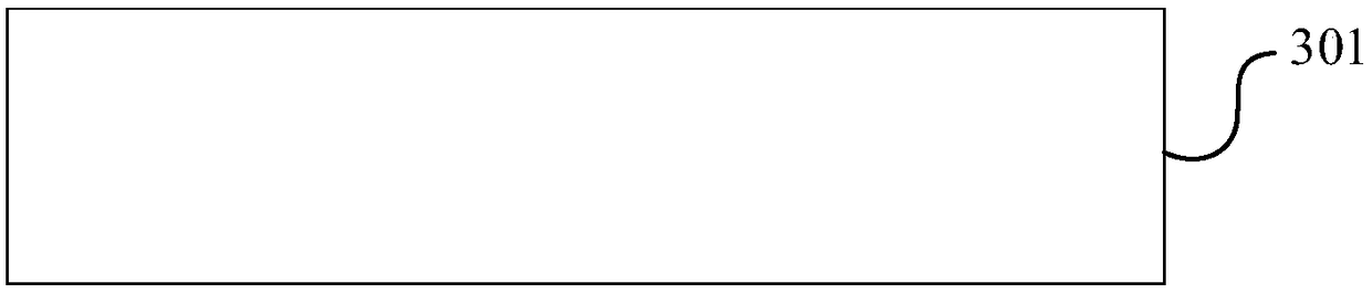
[0095] In this embodiment, on the basis of the foregoing embodiment, specific parameters in the method for preparing the TSV adapter plate of the present invention are described as follows. Specifically, please refer to Figure 3a-Figure 3h , Figure 3a-Figure 3h It is a flowchart of another method for preparing a TSV interposer board for system-in-package provided by an embodiment of the present invention.
[0096] S301. Select Si substrate 301, such as Figure 3a Shown
[0097] Preferably, the doping concentration of the Si substrate is 10 14 ~10 17 cm -3 , The thickness is 150 ~ 250μm.
[0098] S302, such as Figure 3b As shown; using an etching process to prepare three TSV302 on a Si substrate, which may include the following steps:
[0099] S3021, at a temperature of 1050℃~1100℃, grow a layer of 800nm~1000nm SiO on the surface of the Si substrate by thermal oxidation process 2 Floor;
[0100] S3022, using a photolithography process to complete the TSV etching pattern through steps...
PUM
| Property | Measurement | Unit |
|---|---|---|
| Doping concentration | aaaaa | aaaaa |
| Depth | aaaaa | aaaaa |
| Depth | aaaaa | aaaaa |
Abstract
Description
Claims
Application Information