Multi-wavelength silicon-based microcavity laser array and preparation method thereof
A laser array and multi-wavelength technology, applied in the direction of lasers, laser devices, laser components, etc., can solve problems affecting the quality of epitaxial layers, etc., to solve lattice mismatch and thermal mismatch, reduce absorption loss, and reduce loss Effect
- Summary
- Abstract
- Description
- Claims
- Application Information
AI Technical Summary
Problems solved by technology
Method used
Image
Examples
preparation example Construction
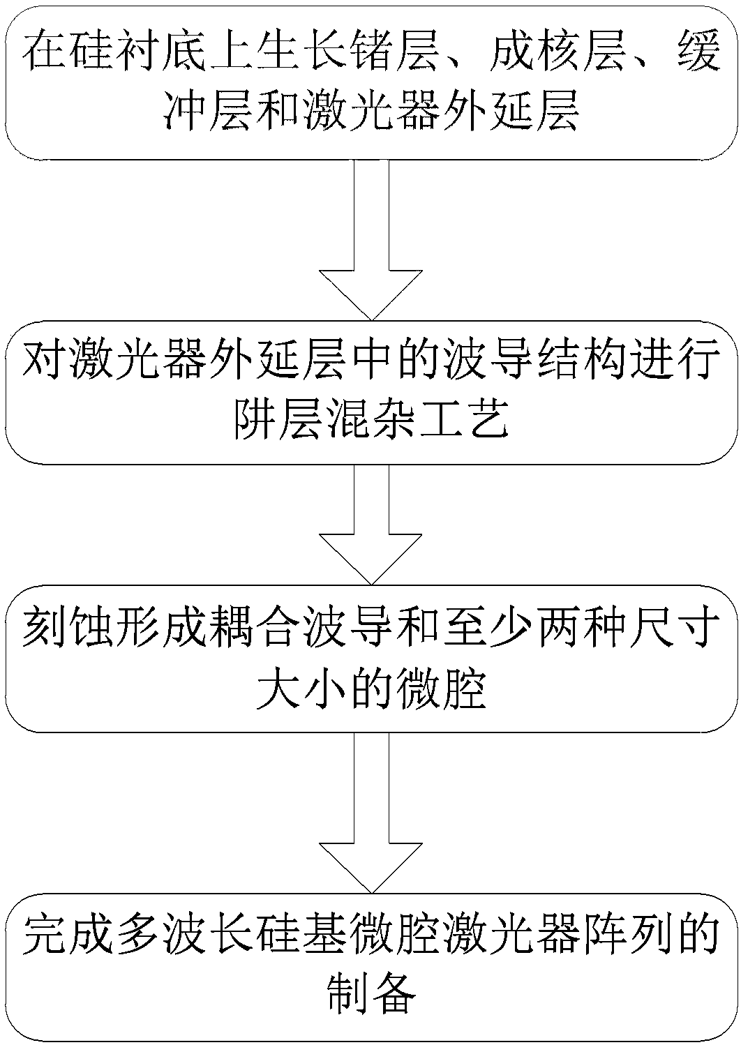
[0036] As a preferred embodiment, the present invention discloses a method for preparing a multi-wavelength silicon-based microcavity laser array, comprising the following steps:
[0037] Step 1, sequentially epitaxially growing a germanium layer, a nucleation layer, a buffer layer and a laser epitaxial layer on a silicon substrate;
[0038] Step 2, performing a well layer hybrid process on the waveguide area outside the light-emitting area in the epitaxial layer of the laser;
[0039] Step 3, etching on the epitaxial layer of the laser to form a coupling waveguide and microcavities of at least two sizes, corresponding to at least two emission wavelengths of the laser array;
[0040] Step 4, depositing a silicon dioxide layer, opening a window, making electrodes, and completing the preparation of a multi-wavelength silicon-based microcavity laser array.
[0041] Wherein, the silicon substrate is an off-cut n-type (100) substrate, which is put into an epitaxial growth reaction...
Embodiment 1
[0053] Such as Figure 1-8 As described, this embodiment provides a method for preparing a multi-wavelength silicon-based microcavity laser array, such as figure 1 As shown, this method includes the following steps:
[0054] Step 1, sequentially epitaxially growing a germanium layer, a nucleation layer, a buffer layer and a laser epitaxial layer on a silicon substrate; this step specifically includes the following sub-steps:
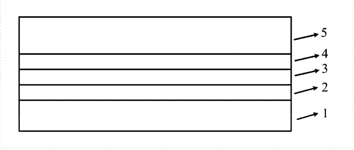
[0055] Step 1-1. Select an N-type low-resistance silicon substrate 1 with an off-cut angle, and put it into an ultra-high vacuum chemical vapor deposition reaction chamber after cleaning a standard silicon wafer;
[0056] Step 1-2, such as figure 2 As shown, the germanium layer 2 is epitaxially grown on the upper surface of the silicon substrate 1 by using the UHVCVD method, which needs to be less than 1×10 6 cm -2 High defect density and surface roughness less than 1nm, and N-type low resistance.
[0057] Step 1-3, such as figure 2 As shown, a g...
Embodiment 2
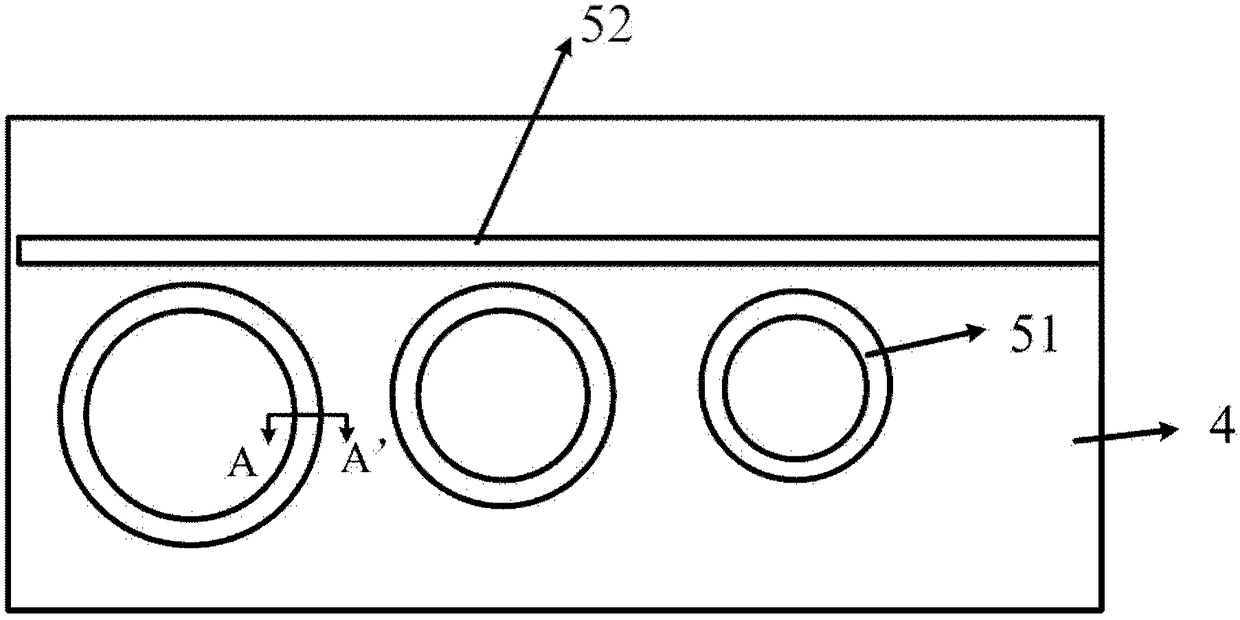
[0068] This embodiment provides a multi-wavelength silicon-based microcavity laser array, such as the cross-sectional view at A-A' Figure 7 As shown, the laser array is described.
[0069] The laser array includes N-type low-resistance silicon-based substrate 1, N-type low-resistance germanium layer 2, gallium arsenide nucleation layer 3, gallium arsenide buffer layer 4, laser epitaxial layer 5 with ridge-table structure, and two layers from bottom to top. The silicon oxide layer 6, the positive electrode 7, and the negative electrode 8 located under the silicon-based substrate 1 are also included.
[0070] Wherein, the upper surface of the laser epitaxial layer 5 has a microcavity with a ring structure etched to the upper surface of the buffer layer and a coupling waveguide with a rectangular parallelepiped structure, and the positive electrode 7 corresponds to the microcavity through an electrode isolation pattern.
[0071] Wherein the silicon dioxide layer 6 has an electr...
PUM
| Property | Measurement | Unit |
|---|---|---|
| Defect density | aaaaa | aaaaa |
| Surface roughness | aaaaa | aaaaa |
| Thickness | aaaaa | aaaaa |
Abstract
Description
Claims
Application Information


