

A low-profile power module for high-frequency applications
A power module, a thin technology, applied in the direction of output power conversion device, AC power input conversion to DC power output, high-efficiency power electronic conversion, etc., can solve problems such as chip breakdown, burning modules, etc.
- Summary
- Abstract
- Description
- Claims
- Application Information
AI Technical Summary
Problems solved by technology
Method used
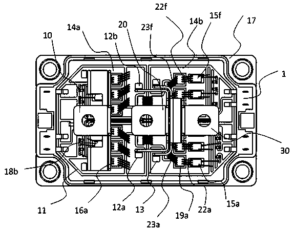
Image

Examples
Embodiment Construction
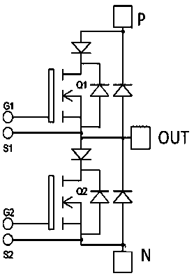
[0020] The present invention is a power module suitable for high-frequency applications. It balances the distributed inductance of the gate control loop and power loop of each chip for wide-bandgap semiconductor chips, such as silicon carbide MOSFETs, so that when the module is turned on, The current borne by each chip is basically balanced, and when the module is turned off, the voltage borne by each chip is also basically balanced. The invention is illustrated with the most common half-bridge power module. Such as figure 1 As shown, the half-bridge power module includes two silicon carbide MOSFET power units, the upper-bridge MOSFET1 and the lower-bridge MOSFET2. In actual operation, the silicon carbide MOSFETs in the upper and lower bridge arms are turned on and off alternately to control the output current. The gate loop of the upper bridge arm is G1-S1, and the gate loop of the lower bridge arm is G2-S2. The corresponding power loop of the upper bridge arm is the posit...
PUM
 Abstract
Description
Claims
Application Information