
HEMT (high electron mobility transistor) device with back field plate structure and preparation method of HEMT device

A back field plate and device technology, used in semiconductor/solid-state device manufacturing, semiconductor devices, electrical components, etc., can solve problems such as thermal breakdown, gate drain side electrical breakdown, silicon substrate breakdown, etc. The effect of breakdown voltage, mitigating electric field peaks, and improving service life

Pending Publication Date: 2018-06-29
SOUTH CHINA UNIV OF TECH
View PDF0 Cites 4 Cited by
  • Summary
  • Abstract
  • Description
  • Claims
  • Application Information

AI Technical Summary

Problems solved by technology

[0005] In order to overcome the above-mentioned shortcomings and deficiencies of the prior art, the object of the present invention is to provide a HEMT device with a back field plate structure, which not only solves the problem that the existing Si substrate HEMT high voltage operation is easy to break down at the silicon substrate, It also solves the problem of electrical breakdown and thermal breakdown on the drain side of the gate, and realizes the normal operation of the Si substrate HEMT at a voltage of 1kV

Method used


Image

  • HEMT (high electron mobility transistor) device with back field plate structure and preparation method of HEMT device

Examples


Embodiment

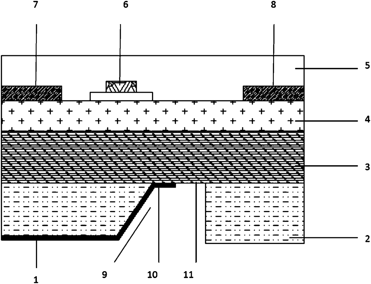
[0027] Such as figure 1 As shown, the HEMT device with the back field plate structure of the present invention includes a silicon substrate 2, a GaN epitaxial layer 3, an AlGaN barrier layer 4, a Si 3 N 4 A passivation protection layer 5; a gate electrode 6, a source electrode 7 and a drain electrode 8 are arranged on the AlGaN barrier layer 4; the silicon substrate is provided with a groove 9 whose cross section is a right-angled trapezoid; Next, the top of the groove is the lower surface of the GaN epitaxial layer; the back field plate structure 1 is set on part of the lower surface of the silicon substrate, the slope of the groove, and part of the top of the groove. The contact line width 10 between the back field plate structure and the GaN epitaxial layer is 5-10 μm. The lateral width of the portion 11 of the groove top not covered by the back field plate structure is 5-10 μm. The back field plate structure is a metal sheet with a thickness of 50nm-2μm.

[0028] A met...


PUM


Abstract

The invention discloses an HEMT (high electron mobility transistor) device with a back field plate structure. The HEMT device comprises a silicon substrate, a GaN epitaxial layer, an AlGaN barrier layer and an Si3N4 passivated protection layer sequentially from bottom to top; a gate electrode, a source electrode and a drain electrode are arranged on the AlGaN barrier layer; a groove with the crosssection in a right trapezoid shape is formed in the silicon substrate; the groove opens downwards, and the top of the groove is the lower surface of the AlGaN barrier layer; a back field plate structure is arranged on part of lower surface of the silicon substrate, the slope of the groove and part of top of the groove. The invention also discloses a preparation method of the HEMT device adoptingthe back field plate structure. By use of substrate isolation and back field plate technologies, substrate breakdown of the device is avoided, the breakdown voltage of the GaN HEMT device is increased, the field intensity peak value of the drain side of the gate electrode is reduced, the cooling performance of the device is improved, and the HEMT device has important significance in realizing high-performance and high-reliability gallium nitride based devices.

Description

technical field [0001] The invention relates to a high electron mobility transistor (HEMT), in particular to a HEMT device with a back field plate structure and a preparation method thereof. Background technique [0002] Power electronic devices are widely used in many fields such as household appliances, industrial equipment, and automotive power supplies. The new generation of power electronic devices requires higher efficiency, higher power density and higher reliability under high temperature working environment. At present, silicon-based power devices, such as MOSFETs and IGBTs, are widely used in power electronic devices. However, after long-term development of silicon electronic power devices, the performance and the theoretical limit of its materials, the new generation of power electronic devices are facing huge challenges such as high voltage, high frequency and small volume. The third-generation semiconductor material GaN has the advantages of large band gap, hi...

Claims


Application Information

Patent Timeline
Patent Type & Authority Applications(China)
IPC IPC(8): H01L29/778H01L21/335H01L29/40
CPCH01L29/402H01L29/66462H01L29/7783
Inventor 李国强陈丁波刘智崑万利军
Owner SOUTH CHINA UNIV OF TECH
Learn More