SiC-based DI-MOSFET preparation method and SiC-based DI-MOSFET

A technology of substrate and ion implantation area, applied in semiconductor/solid-state device manufacturing, electrical components, circuits, etc., can solve problems such as limiting device switching speed, large gate-to-drain capacitance, increasing device switching loss, etc., to reduce dynamic loss, The effect of reducing gate-drain capacitance and increasing operating frequency

Inactive Publication Date: 2018-07-06
BEIJING PINJIE ELECTRONICS TECH CO LTD
View PDF6 Cites 2 Cited by
  • Summary
  • Abstract
  • Description
  • Claims
  • Application Information

AI Technical Summary

Problems solved by technology

Since the gate and the SiC epitaxial layer are only separated by a thin gate oxide layer, the gate-to-drain capacitance is relatively large, which limits the switching speed of the device and increases the switching loss of the device.

Method used


Image

  • SiC-based DI-MOSFET preparation method and SiC-based DI-MOSFET
  • SiC-based DI-MOSFET preparation method and SiC-based DI-MOSFET
  • SiC-based DI-MOSFET preparation method and SiC-based DI-MOSFET

Examples


Embodiment 1

[0037] This embodiment provides a method for preparing a SiC-based DI-MOSFET, such as figure 1 Shown, this preparation method comprises the steps:

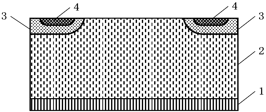
[0038] S1: Select the SiC epitaxial substrate obtained after epitaxially growing a SiC epitaxial layer 2 on the front side of the SiC substrate 1, such as figure 2 shown;

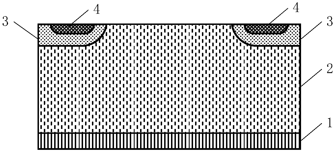
[0039] S2: Implanting p-type ions into a part of the surface of the SiC epitaxial layer 2 using a photolithography mask to form two p-type ion implantation regions 3; and then implanting into a part of the surface of each p-type ion implantation region 3 using a photolithography mask N-type ions form an n-type ion implantation region 4 in each p-type ion implantation region 3; the implanted p-type ions and n-type ions are activated by an annealing, such as image 3 shown;

[0040] S3: using a photolithographic mask to implant oxygen ions into a part of the surface of the SiC epitaxial layer 2 located between the two p-type ion implantation regions 3 to form...


PUM


Abstract

The invention discloses a SiC-based DI-MOSFET preparation method and the SiC-based DI-MOSFET. The SiC-based DI-MOSFET comprises a SiC epitaxial substrate, two p-type ion implantation regions (3) and two n-type ion implantation regions (4) formed on the surface of a SiC epitaxial layer (2), an oxide layer (6), a grid (7) covering the surface of the oxide layer (6), a dielectric layer (8) wrapping the grid (7), a source metal layer (9) covering surfaces of two source contact holes and the dielectric layer (8), and a drain metal layer (10) covering the back surface of a SiC substrate (1), whereineach n-type ion implantation region (4) is arranged in each p-type ion implantation region (3), thickness of the oxide layer (6) between the two p-type ion implantation regions (3) is greater than thickness of the oxide layer (6) at other regions, two sides of the dielectric layer (8) are respectively provided with one source contact hole, and the drain metal layer (10) and the SiC substrate (1)are in ohmic contact. The SiC-based DI-MOSFET is advantaged in that gate leakage capacitance of devices can be reduced.

Description

technical field [0001] The invention belongs to the field of semiconductor devices, and in particular relates to a preparation method of a SiC-based DI-MOSFET and the SiC-based DI-MOSFET. Background technique [0002] Silicon carbide (Silicon Carbide, SiC) is an excellent wide-bandgap semiconductor material, which has the advantages of high critical breakdown electric field strength, high saturation electron mobility, and high thermal conductivity. Power electronic devices based on SiC can achieve higher conversion efficiency, higher operating frequency and lower power loss than silicon-based devices of the same electrical level. The SiC-based switching device is mainly DI-MOSFET (Double Implanted Metal Oxide Semiconductor FieldEffect Transistor). This device mainly forms p-type doped regions and n-type doped regions through two ion implantations and high-temperature annealing to activate impurities. Then, a gate oxide layer is formed on the surface of SiC by thermal oxygen...

Claims


Application Information

Patent Timeline
Patent Type & Authority Applications(China)
IPC IPC(8): H01L21/336H01L29/06H01L29/78
CPCH01L29/0653H01L29/66068H01L29/7827
Inventor 何志
Owner BEIJING PINJIE ELECTRONICS TECH CO LTD
Why Eureka
Try Eureka