Eureka AIR delivers breakthrough ideas for toughest innovation challenges, trusted by R&D personnel around the world.

A kind of Gan base enhanced field effect device and its manufacturing method

An enhanced, field-effect technology, applied in semiconductor/solid-state device manufacturing, semiconductor devices, electrical components, etc., can solve problems such as barrier layer surface damage, achieve good threshold consistency, low interface state, and high hole concentration Effect

Active Publication Date: 2020-09-29
INST OF MICROELECTRONICS CHINESE ACAD OF SCI
View PDF4 Cites 3 Cited by
  • Summary
  • Abstract
  • Description
  • Claims
  • Application Information

AI Technical Summary

Problems solved by technology

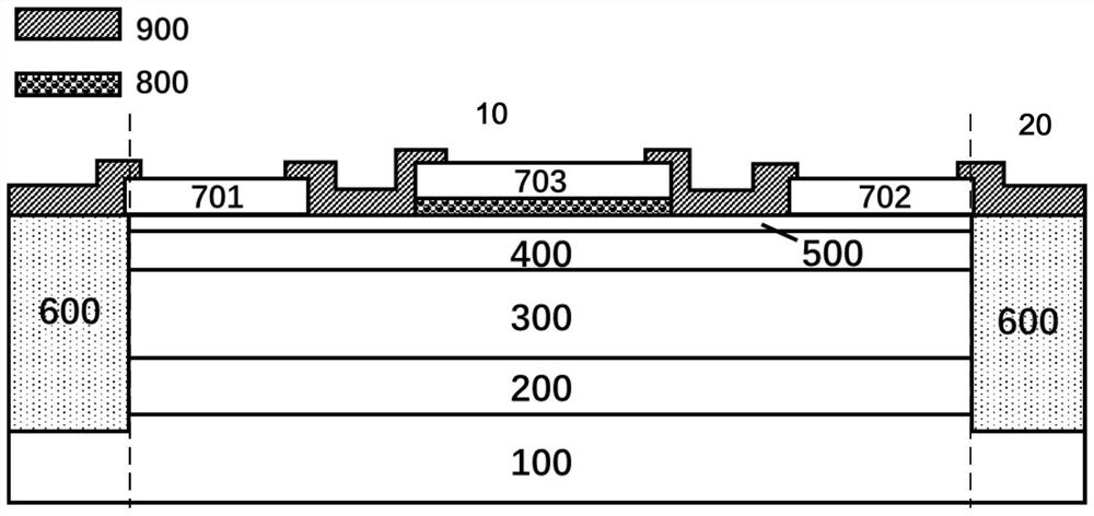
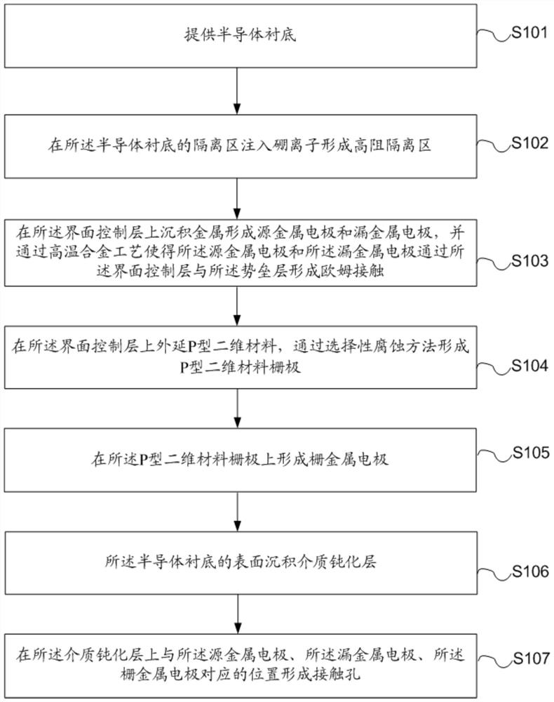
[0005] In view of this, the present invention provides a GaN-based enhancement type field effect device and its manufacturing method to solve the problem of barrier layer caused by dry etching when growing a single-layer p-GaN capping layer on the gate in the prior art. The problem of surface damage

Method used


Image

  • A kind of Gan base enhanced field effect device and its manufacturing method
  • A kind of Gan base enhanced field effect device and its manufacturing method
  • A kind of Gan base enhanced field effect device and its manufacturing method

Examples


Embodiment Construction

[0037] As mentioned in the background technology section, the GaN-based enhancement field effect device method in the prior art has various disadvantages, and GaN-based enhancement field effect devices with good process consistency cannot be obtained.

[0038] The inventors found that the reason for the above problems is that a single layer of p-GaN capping layer or p-AlGaN capping layer is grown under the gate in GaN-based enhancement field effect devices in the prior art, but due to the p-GaN material , resulting in a low doping concentration of P-type impurities, and it is mostly formed by dry etching process, which is easy to cause damage on the surface of the barrier layer, so that a GaN-based enhancement mode field effect device with good process consistency cannot be obtained.

[0039] Based on this, the present invention provides a GaN-based enhanced field effect device, including: an active region and an isolation region surrounding the active region, the active region...


PUM

PropertyMeasurementUnit
thicknessaaaaaaaaaa

Abstract

The invention provides a GaN-based enhanced field effect device and a manufacturing method thereof. The GaN-based enhanced field effect device comprises an active region and an isolation region surrounded by the active region, wherein the active region comprises a single crystal substrate, a buffer layer, a channel layer, a barrier layer, an interface control layer, a source metal electrode, a drain metal electrode, a grid metal electrode and a dielectric passivation layer and further comprises a P-type two-dimensional material grid; the P-type two-dimensional material grid is inserted below the grid metal electrode, so the two-dimensional electron gas in the channel below the grid can be effectively depleted, and the GaN-based enhanced field effect device is realized. The P-type two-dimensional material is advantaged in that cavity concentration is high, crystal lattice matching and a low interface state are realized, selective removal from the surface of a gallium nitride material can be realized, and process controllability is good, so threshold consistency of the acquired GaN-based enhanced field effect device is good, and a reliability problem caused by current collapse is well suppressed.

Description

technical field [0001] The invention relates to the field of manufacturing semiconductor devices, in particular to a GaN-based enhanced field effect device and a manufacturing method thereof. Background technique [0002] GaN materials have the characteristics of large band gap, high critical breakdown electric field, and high thermal conductivity, and have broad application prospects in broadband communications, power electronics, and other fields. Due to the spontaneous polarization and piezoelectric polarization effects at the interface between gallium nitride (GaN) and aluminum gallium nitride (AlGaN) heterojunction, the two-dimensional electron gas concentration is very high (>1E13cm -2 ), which makes GaN field effect devices, that is, HEMT (High Electron Mobility Transistor, high electron mobility transistor) devices, have very low on-resistance and switching delay. However, the high concentration of two-dimensional electron gas at the AlGaN / GaN heterointerface mak...

Claims


Application Information

Patent Timeline
Patent Type & Authority Patents(China)
IPC IPC(8): H01L29/423H01L29/47H01L29/49H01L29/778H01L21/335H01L21/28
CPCH01L29/42312H01L29/47H01L29/4908H01L29/66462H01L29/7787
Inventor 刘洪刚黄凯亮常虎东
Owner INST OF MICROELECTRONICS CHINESE ACAD OF SCI
Why Eureka
Eureka Blog
Learn More