Wafer level GaN device substrate transfer method

A substrate transfer, wafer-level technology, applied in semiconductor/solid-state device manufacturing, electrical components, circuits, etc., can solve problems such as performance degradation

Active Publication Date: 2018-07-17
BEIJING HUATAN TECH CO LTD
View PDF3 Cites 6 Cited by
  • Summary
  • Abstract
  • Description
  • Claims
  • Application Information

AI Technical Summary

Problems solved by technology

[0006] The object of the present invention is to provide a method for substrate transfer of a wafer-level GaN device, through surface spin-coating thicker photosensitive BCB, and then forming a surface-activated bonding method of a protective support layer, to achieve on a heterogeneous substrate ( The substrate transfer

Method used


Image

  • Wafer level GaN device substrate transfer method
  • Wafer level GaN device substrate transfer method
  • Wafer level GaN device substrate transfer method

Examples


Embodiment 1

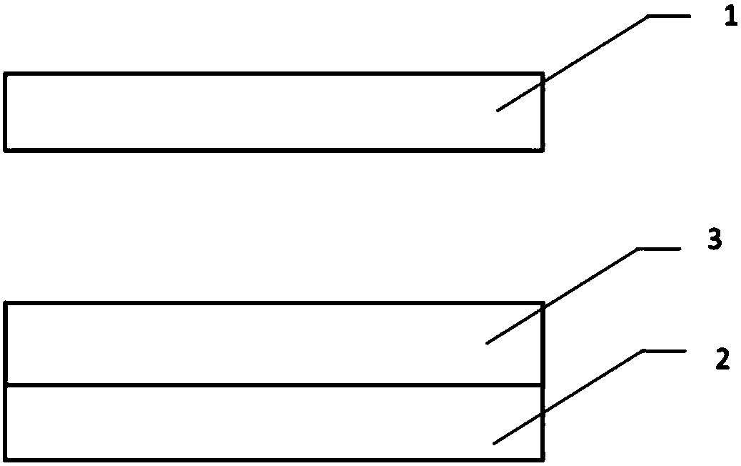
[0037] Such as Figure 1~5 As shown, according to the wafer bonding method implemented in the present invention, the method includes the following steps:

[0038] Step 1: After the front-side process of wafer-level GaN device 3 is completed, spin-coat photosensitive BCB4 on the surface of the wafer, set the rotation speed to 1000rpm, and take 1min; place the GaN device wafer on a hot plate and heat it to remove the solvent in the BCB glue , The heating temperature is kept at 100 ℃ ~ 200 ℃ to prevent the BCB glue from being removed after the transfer is completed due to high temperature BCB curing. figure 1 It is a schematic diagram of the cross-section of the wafer before bonding, figure 2 Schematic diagram of the cross-section of a spin-coated photosensitive BCB on the surface of a GaN device after the front-side process is completed.

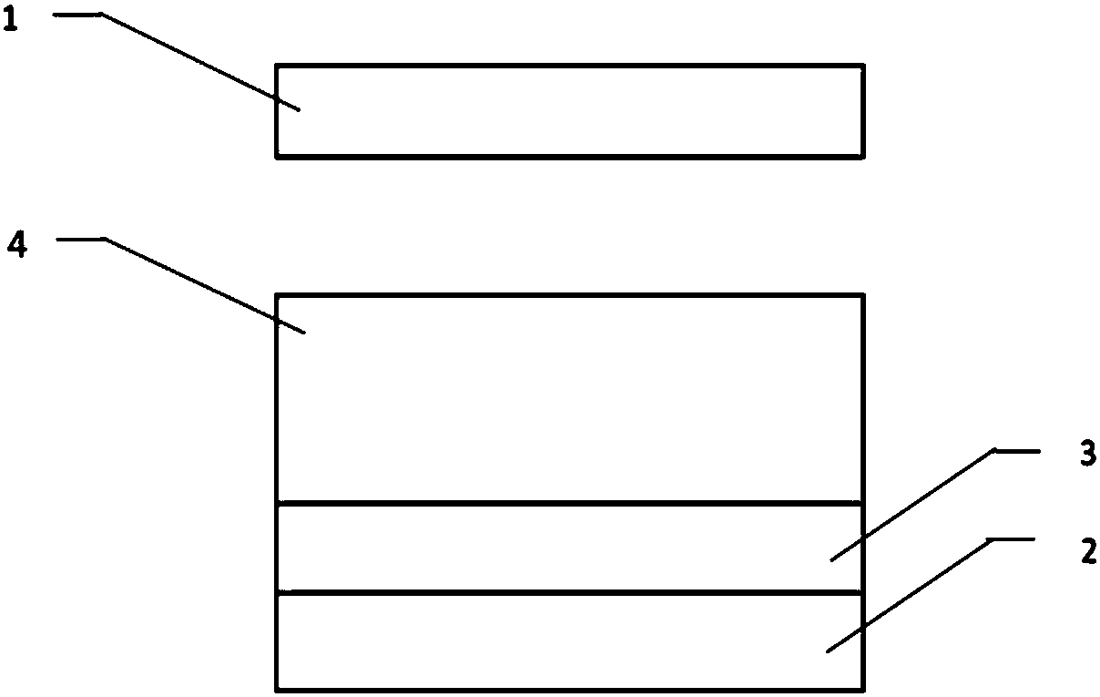
[0039] Step 2: The sapphire substrate 2 is peeled off by a KrF excimer laser.

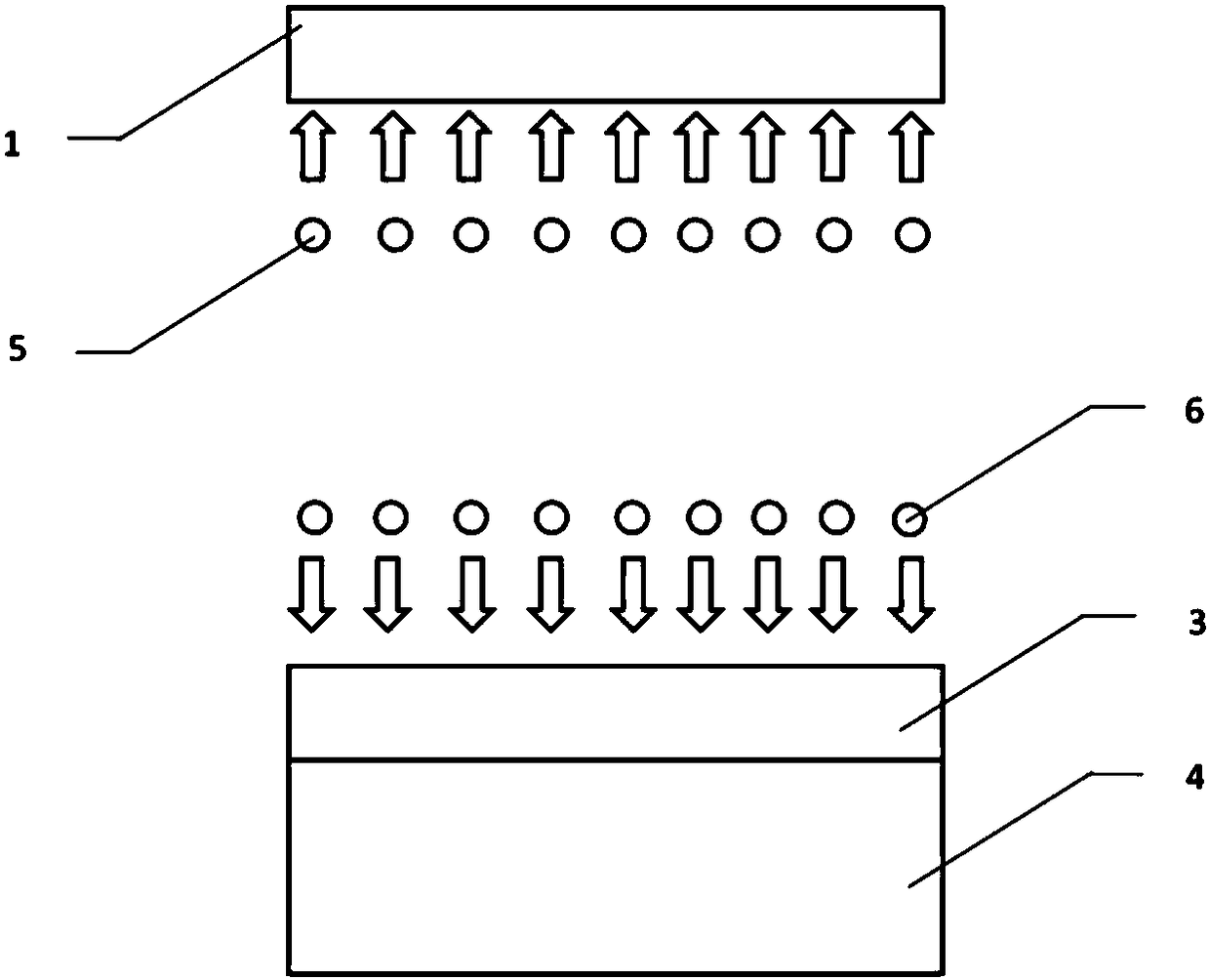
[0040] Step 3: Cleaning the Si wafer 1 and the GaN device...

Embodiment 2

[0048] Step 1: After the front-side process of wafer-level GaN device 3 is completed, spin-coat photosensitive BCB4 on the surface of the wafer, set the rotation speed to 1000rpm, and take 1min; place the GaN device wafer on a hot plate and heat it to remove the solvent in the BCB glue , The heating temperature is kept at 100°C to prevent the high-temperature BCB from curing and the BCB glue cannot be removed after the transfer is completed. figure 1 It is a schematic diagram of the cross-section of the wafer before bonding, figure 2 Schematic diagram of the cross-section of a spin-coated photosensitive BCB on the surface of a GaN device after the front-side process is completed.

[0049] Step 2: removing the SiC substrate or Si substrate on which the heteroepitaxially grown GaN is grown;

[0050] Step 3: Cleaning the Si wafer 1 and the GaN device wafer 3 after removing the substrate by standard RCA. Specifically, when the surface roughness of the wafer is large (usually gr...


PUM

PropertyMeasurementUnit
Thicknessaaaaaaaaaa

Abstract

The invention discloses a transfer method based on a wafer level GaN device original substrate, and belongs to the technical field of semiconductor technology. The surface of an original film is covered with a removable thicker protection supporting layer, and after the original substrate is removed, two wafers are bonded directly. The method comprises the following steps: (1) enabling the surfaceof a wafer level GaN device after front face technology to be covered with the protection supporting layer; (2) removing the original substrate; (3) cleaning the back face of a wafer and the surfaceof an Si substrate to be transferred; (4) carrying out N2 gas plasma processing on the back face of the wafer; (5) carrying out O2 gas plasma processing on the surface of the Si wafer; (6) putting thetwo parts into an ammonia water solution for prebonding; (7) applying external force to a laminated sample in an N2 environment for bonding; (8) carrying out low temperature annealing processing on the bonded wafer; (9) exposing the annealed wafer, and then putting the exposed wafer into a developing solution to resolve and remove a surface protective layer. According to the method, the substratetransfer of the GaN device can be realized.

Description

technical field [0001] The invention belongs to the technical field of semiconductor technology, and in particular relates to a method for substrate transfer of a wafer-level GaN device. Background technique [0002] Gallium nitride (GaN) is a very attractive material for high power and high frequency devices such as high electron mobility transistors (HEMTs) due to their high electron saturation velocity and wide bandgap. Currently, epitaxial GaN can be grown on heterogeneous substrates such as silicon (Si), sapphire (Al 2 o 3 ) or silicon carbide (SiC) and on homogeneous substrates. GaN grown on Si is most preferred because Si wafers are available in larger diameters and have higher thermal conductivity than sapphire. However, the quality of epitaxial GaN grown on Si is limited due to high threading dislocation density (TDD) and cracks due to large thermal and lattice mismatch, which lead to poor device performance and low yield . [0003] Recently, several epitaxial ...

Claims


Application Information

Patent Timeline
IPC IPC(8): H01L21/18
CPCH01L21/187
Inventor 梁世博
Owner BEIJING HUATAN TECH CO LTD
Why Eureka
Try Eureka