Supercharge Your Innovation With Domain-Expert AI Agents!

Tungsten silicide nitride films and methods of formation

A technology of tungsten nitride layer and silicon nitride, which is applied in the direction of vacuum evaporation plating, coating, transistor, etc., can solve the problems of inability to provide gate stack resistivity, unsatisfactory adhesion, etc.

Inactive Publication Date: 2018-07-17
APPLIED MATERIALS INC
View PDF6 Cites 1 Cited by
  • Summary
  • Abstract
  • Description
  • Claims
  • Application Information

AI Technical Summary

Problems solved by technology

However, the inventors have observed that the adhesion layer often exhibits unsatisfactory adhesion to the underlying oxide and subsequently deposited bulk tungsten, and also fails to provide suitable resistivity for the gate stack.

Method used


Image

  • Tungsten silicide nitride films and methods of formation
  • Tungsten silicide nitride films and methods of formation
  • Tungsten silicide nitride films and methods of formation

Examples


Embodiment Construction

[0013] The present disclosure relates to tungsten silicide films and methods of depositing tungsten silicide films. In at least some embodiments, the inventive films and methods described herein beneficially reduce or eliminate spalling of the tungsten that is deposited to form a gate electrode stack of tungsten while maintaining a suitable gate stack resistivity, and Substantially neutral substrate stress is maintained.

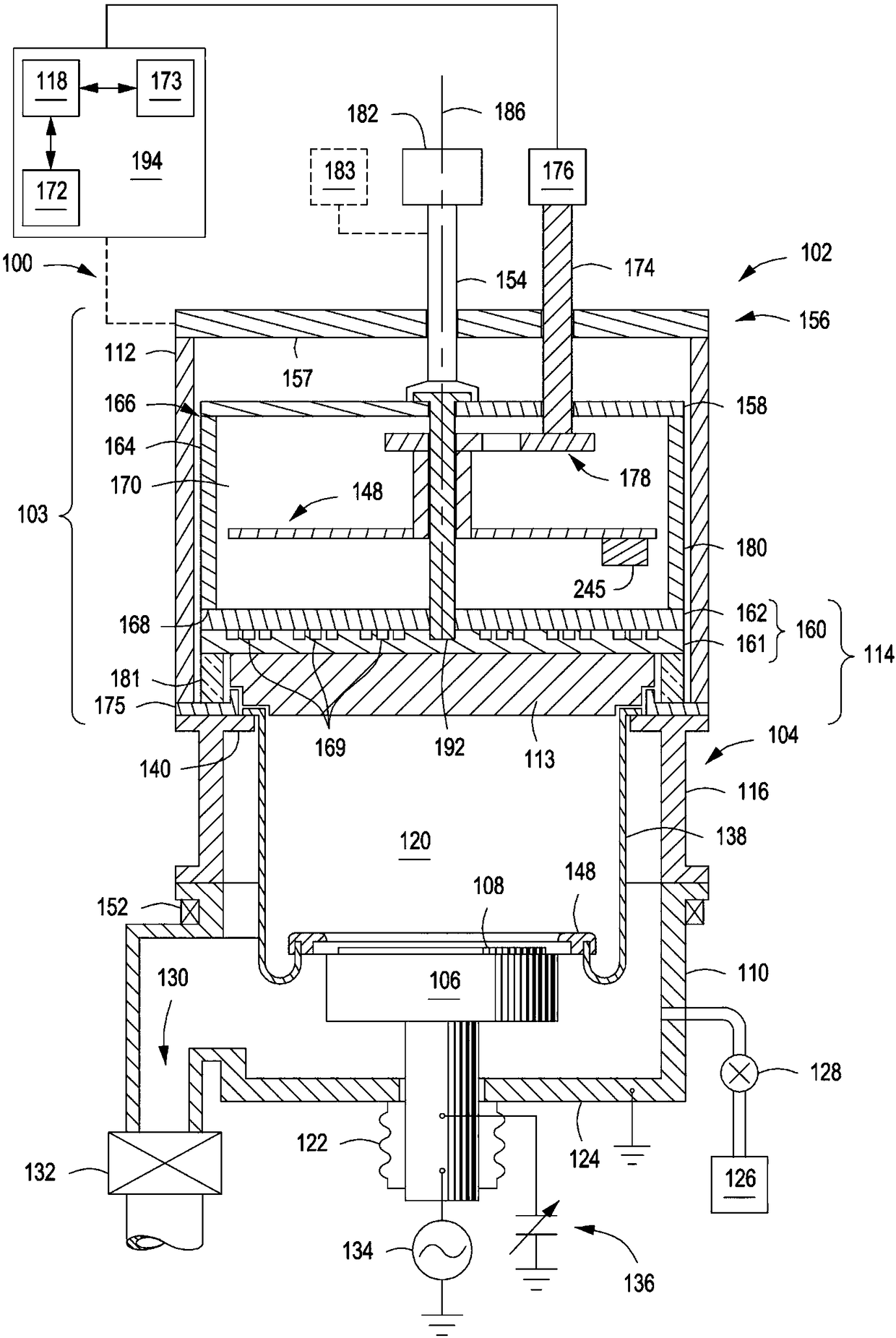
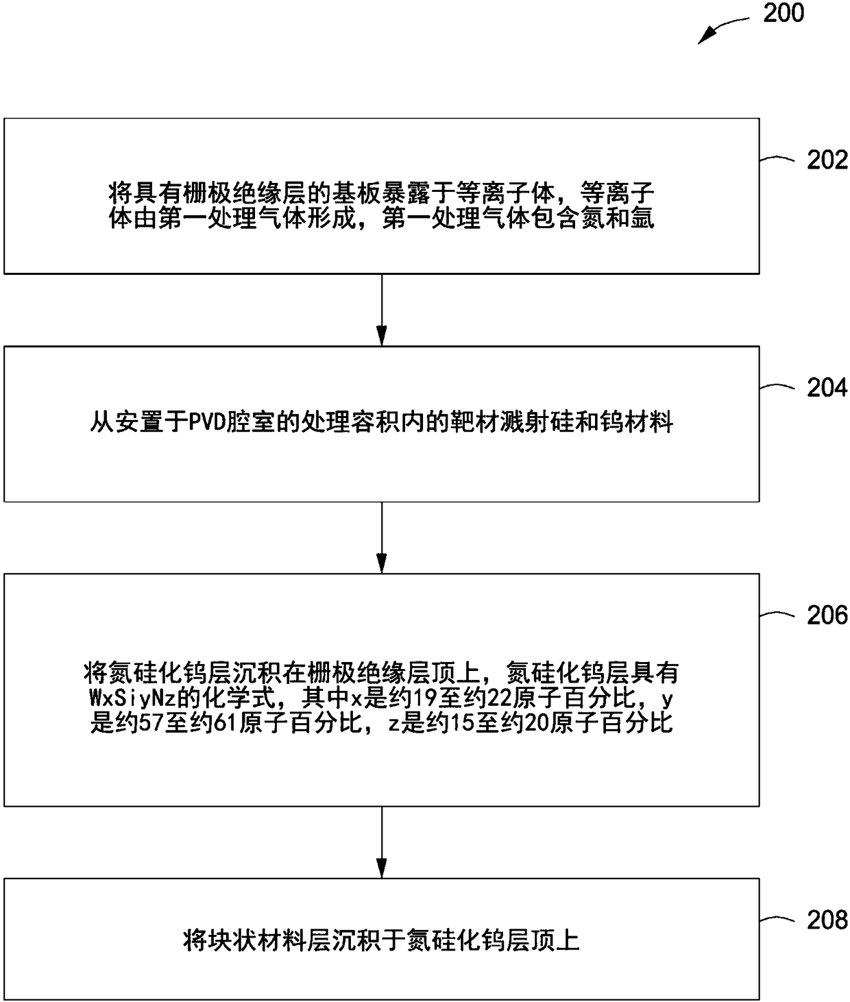
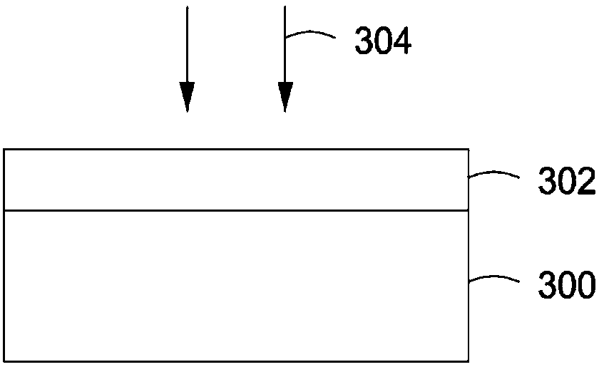
[0014] According to some embodiments of the present disclosure, figure 1 A simplified cross-sectional view of an illustrative physical vapor deposition (PVD) processing system 100 is depicted. figure 2 A flow chart depicting a method 200 of depositing a dielectric layer atop a substrate positioned such as figure 1 The type of physical vapor deposition processing system. hereinafter related to Figure 3A to Figure 3D The depicted stages of processing a substrate describe method 200 . An example of a PVD chamber suitable for performing the method 200 des...


PUM

PropertyMeasurementUnit
thicknessaaaaaaaaaa
thicknessaaaaaaaaaa
lengthaaaaaaaaaa

Abstract

Embodiments of the present invention include tungsten silicide nitride films and methods for depositing tungsten silicide nitride films. In some embodiments, a thin film microelectronic device includes a semiconductor substrate having a tungsten gate electrode stack comprising a tungsten silicide nitride film having a formula WxSiyNz, wherein x is about 19 to about 22 atomic percent, y is about 57to about 61 atomic percent, and z is about 15 to about 20 atomic percent. In some embodiments, a method of processing a substrate disposed in physical vapor deposition (PVD) chamber, includes: exposing a substrate having a gate insulating layer to a plasma formed from a first process gas comprising nitrogen and argon; sputtering silicon and tungsten material from a target disposed within a processing volume of the PVD chamber; depositing atop the gate insulating layer a tungsten silicide nitride layer as described above; and depositing a bulk tungsten layer atop the tungsten silicide nitridelayer.

Description

technical field [0001] Embodiments of the present disclosure relate generally to substrate processing systems and methods, and, more particularly, to tungsten nitride suicide films and methods of depositing tungsten nitride suicide films. Background technique [0002] Tungsten (W) is frequently used as a gate conductor material in the fabrication of integrated circuits including dynamic random access memory (DRAM). However, integrating tungsten into semiconductor processing involves several significant challenges. For example, the fabrication of a typical tungsten gate electrode stack involves forming a gate oxide layer on a silicon substrate, eg, by thermal oxidation or chemical vapor deposition (CVD). Subsequent deposited bulk tungsten films have relatively poor adhesion to the gate oxide layer. Therefore, prior to the deposition of the bulk tungsten film, an adhesion layer (ie glue layer), such as tungsten silicide (WSi) or tungsten nitride (WN), is deposited on the gat...

Claims


Application Information

Patent Timeline
Patent Type & Authority Applications(China)
IPC IPC(8): H01L21/285H01L21/28H01L27/108
CPCH01L21/28097H01L21/28202C23C14/0036C23C14/022C23C14/0641H01L29/4975H01L21/2855H01L21/28194H01L21/28556H01L2924/01074H10B12/00H01L21/28088
Inventor 乔斯林甘·罗摩林甘拉尹库曼·雅卡尔尤雷建新王志勇
Owner APPLIED MATERIALS INC
Features
  • R&D
  • Intellectual Property
  • Life Sciences
  • Materials
  • Tech Scout
  • Unparalleled Data Quality
  • Higher Quality Content
  • 60% Fewer Hallucinations
Learn More