
Three-dimensional photoelectric integrated filter realized based on CMOS post-process and preparation method thereof

A photoelectric integration and filter technology, which is applied in the direction of electrical solid-state devices, semiconductor/solid-state device manufacturing, circuits, etc., can solve the problems of center wavelength drift, very strict working temperature requirements, and sensitivity to temperature changes, and achieve the effect of improving bandwidth

Active Publication Date: 2018-07-24
INST OF SEMICONDUCTORS - CHINESE ACAD OF SCI
View PDF4 Cites 4 Cited by
  • Summary
  • Abstract
  • Description
  • Claims
  • Application Information

AI Technical Summary

Problems solved by technology

The advantage of the multiplexer and demultiplexer based on the microring filter is small size and easy on-chip integration. The disadvantage is that it is extremely sensitive to temperature changes and has very strict requirements on the working temperature. A small temperature drift will lead to a drift of the center wavelength.

Method used


Image

  • Three-dimensional photoelectric integrated filter realized based on CMOS post-process and preparation method thereof
  • Three-dimensional photoelectric integrated filter realized based on CMOS post-process and preparation method thereof
  • Three-dimensional photoelectric integrated filter realized based on CMOS post-process and preparation method thereof

Examples


Embodiment Construction

[0041] In order to make the object, technical solution and advantages of the present invention clearer, the present invention will be further described in detail below in conjunction with specific embodiments and with reference to the accompanying drawings.

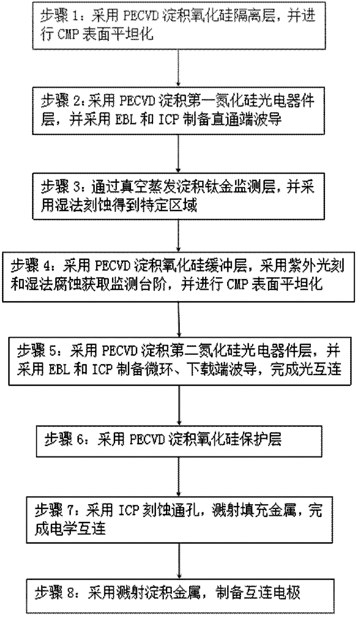
[0042] The present invention proposes a three-dimensional photoelectric integrated filter based on post-CMOS technology. All process temperatures are controlled below 400°C to avoid impact on the CMOS integrated circuit, realize single-chip integration of photoelectric devices and CMOS integrated circuits, and simultaneously realize three-dimensional optical Interconnection solves the bottleneck problem of electrical interconnection.

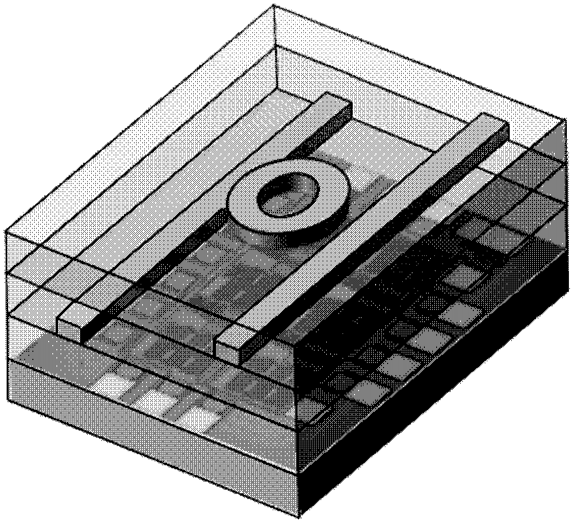
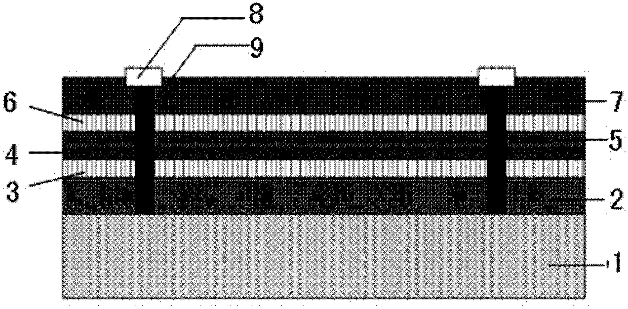
[0043] refer to figure 1 and figure 2 , the present invention is based on the three-dimensional optoelectronic integrated filter realized by the post-CMOS process, including the silicon oxide isolation layer 2, the first silicon nitride optoelectronic device layer 3, and the titanium gold...


PUM


Abstract

The invention provides a three-dimensional photoelectric integrated filter and a preparation method thereof. The three-dimensional photoelectric integrated filter comprises an isolation layer, a firstphotoelectric device layer, a monitoring layer, a buffer layer, a second photoelectric device layer and a protection layer, which are deposited on a CMOS integrated circuit in sequence from the bottom up. A plurality of through holes pass through the layers above. Each through hole is filled with metal, which makes contact with an electrode of the CMOS integrated circuit. An interconnection electrode is arranged above each through hole. The first photoelectric device layer is used for preparing a lower filter interacting with the CMOS integrated circuit; and the second photoelectric device layer is used for preparing an upper filter for optical interconnection with the first photoelectric device layer. The three-dimensional photoelectric integrated filter not only can solve the problem ofloss and crosstalk of optoelectronic integrated optical interconnection in a single plane, realizes multidimensional optoelectronic integration in a plurality of planes and improves the density of photoelectron integration and the complexity of an optical interconnection system, but also can solve the problem of dependency of a microloop filter on environment temperature; and through automatic thermal tuning of a bottom temperature control circuit for the upper filter, a purpose of wide operating temperature range is realized.

Description

technical field [0001] The invention relates to the technical field of optoelectronic integration, in particular to a three-dimensional optoelectronic integrated filter based on post-CMOS technology and a preparation method thereof. Background technique [0002] With the continuous development of integrated circuit technology in the direction of high speed and high integration, Moore's Law is facing the ultimate challenge of chip integration. Traditional electrical interconnection inevitably has problems such as high delay, high power consumption, and severe signal crosstalk. So people turned their attention to a new generation of interconnection technology - optical interconnection. Optical interconnection has the advantages of wide bandwidth, anti-electromagnetic interference, strong confidentiality, low loss and low power consumption, while silicon-based optical interconnection can play the advantages of wide bandwidth, low crosstalk, low loss and compatibility with CMOS ...

Claims


Application Information

Patent Timeline
Patent Type & Authority Applications(China)
IPC IPC(8): H01L21/82H01L21/8238H01L27/085H01L27/12
CPCH01L21/82H01L21/8238H01L27/085H01L27/12
Inventor 黄北举张欢程传同陈弘达
Owner INST OF SEMICONDUCTORS - CHINESE ACAD OF SCI
Learn More