Grinding and cutting method for chip of low-channel arrayed waveguide grating wavelength division multiplexer

An arrayed waveguide grating and wavelength division multiplexer technology, applied in the field of optical communication, can solve the problems of high angle defect rate, high product scrap rate, low rework efficiency, etc., to facilitate grinding and polishing, improve detection efficiency, and rework efficiency. high effect

Active Publication Date: 2018-08-07
WUHAN YILUT TECH CO LTD
View PDF7 Cites 5 Cited by
  • Summary
  • Abstract
  • Description
  • Claims
  • Application Information

AI Technical Summary

Problems solved by technology

Due to the small size of a single chip, the angle defect rate after grinding the input end face and the output end face is high, and a single chip is reworked one by one, the rework efficiency is low, and the scrap rate of the whole process is high; The upper surface of the silicon-based chip is not covered with a glass cover, and the edge chipping and crack defect rate is high during the grinding process of the output end face, and the product scrap rate is high

Method used


Image

  • Grinding and cutting method for chip of low-channel arrayed waveguide grating wavelength division multiplexer
  • Grinding and cutting method for chip of low-channel arrayed waveguide grating wavelength division multiplexer
  • Grinding and cutting method for chip of low-channel arrayed waveguide grating wavelength division multiplexer

Examples


Embodiment

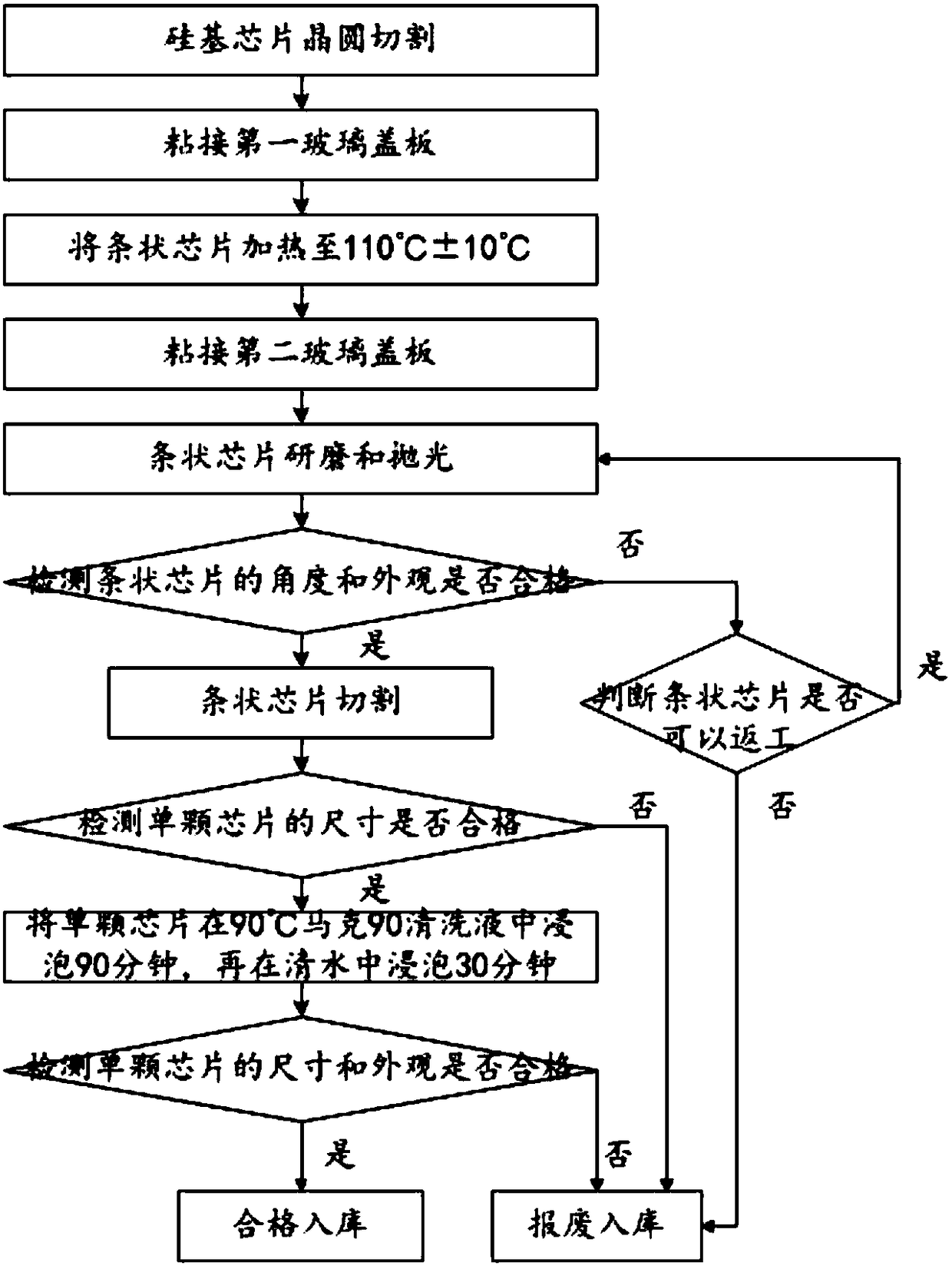
[0045] Example: Grinding and cutting of four-channel arrayed waveguide grating wavelength division multiplexer chip

[0046] Step 1. Cut the silicon-based chip wafer into strip chips. The width of the strip chip is 8.6-9.2 mm, the length of a single four-channel arrayed waveguide grating wavelength division multiplexer chip. The length of the strip chip is The value is greater than or equal to twice the width of a single four-channel arrayed waveguide grating wavelength division multiplexer chip 1.4 ~ 1.75mm, and the height of the strip chip is equal to or greater than that of a single four-channel arrayed waveguide grating wavelength division multiplexer chip Including the height of the glass cover 1mm;

[0047] Step 2: Use UV glue to bond the first glass cover with the same length as the strip chip, less than 0.9-1.1mm in width, and 0.138-0.142mm in height to the left end of the upper surface of the strip chip, as shown in figure 2 shown;

[0048] Step 3, heating the stri...


PUM

PropertyMeasurementUnit
lengthaaaaaaaaaa
widthaaaaaaaaaa
heightaaaaaaaaaa

Abstract

The invention relates to a grinding and cutting method for a chip of a low-channel arrayed waveguide grating wavelength division multiplexer. According to the method, the two end surfaces in the widthdirection of strip-shaped chips are ground and polished on a grinding machine until different preset angles are formed between the two end surfaces of each strip-shaped chip and the upper surface ofa first glass cover plate, and therefore the different preset angles can be formed between the input end surface and the output end surface of one chip and the upper surface of one first glass cover plate; the size of each strip-shaped chip is relatively large, so that grinding and polishing are facilitated, and in addition, angle detection is carried out on the two end surfaces in the width direction of the strip-shaped chips, namely, angle detection can be simultaneously carried out on the input end surfaces and the output end surfaces of the multiple chips, so that the detection efficiencycan be improved; in addition, if the strip-shaped chips are unqualified in angle detection, reworking is needed, the overall reworking can be carried out, and the reworking efficiency is high; and inthe grinding process of the strip-shaped chips, the upper surfaces of the silicon-based chips are covered with the glass cover plates, the glass cover plates play a certain protection role on the silicon-based chips, and therefore the reject ratio caused by edge breakage, cracks and the like in the grinding process can be effectively lowered.

Description

technical field [0001] The invention relates to the technical field of optical communication, in particular to a grinding and cutting method for a low-channel arrayed waveguide grating wavelength division multiplexer chip. Background technique [0002] With the development of communication services and the surge of transmission capacity, CWDM (Coarse Wavelength Division Multiplexing System) has attracted more and more attention. CWDM, which was applied to the backbone network in North America in the early stage, has been rapidly promoted to the whole world, and is widely used in the metropolitan area network. At present, there are three main types of CWDM technologies developed at home and abroad, which are based on arrayed waveguide grating, dielectric film filter and fiber grating technology. Arrayed waveguide grating is a planar waveguide device, which is fabricated on a chip substrate by using PLC technology. At present, compared with dielectric film filters and fiber ...

Claims


Application Information

Patent Timeline
Patent Type & Authority Applications(China)
IPC IPC(8): B24B37/00B28D5/00
CPCB24B37/00B28D5/00
Inventor 李家喻邱志英
Owner WUHAN YILUT TECH CO LTD
Why Eureka
Try Eureka