Method for preparing porous nano-copper structure
A technology of nano-copper and copper target, which is applied in the direction of nanotechnology, nanotechnology, nanotechnology for materials and surface science, etc. It can solve the problems that metal copper is easy to be oxidized, and the research on decomposition products is less in-depth and detailed. , to avoid oxidation
- Summary
- Abstract
- Description
- Claims
- Application Information
AI Technical Summary
Problems solved by technology
Method used
Image

Examples
Embodiment 1
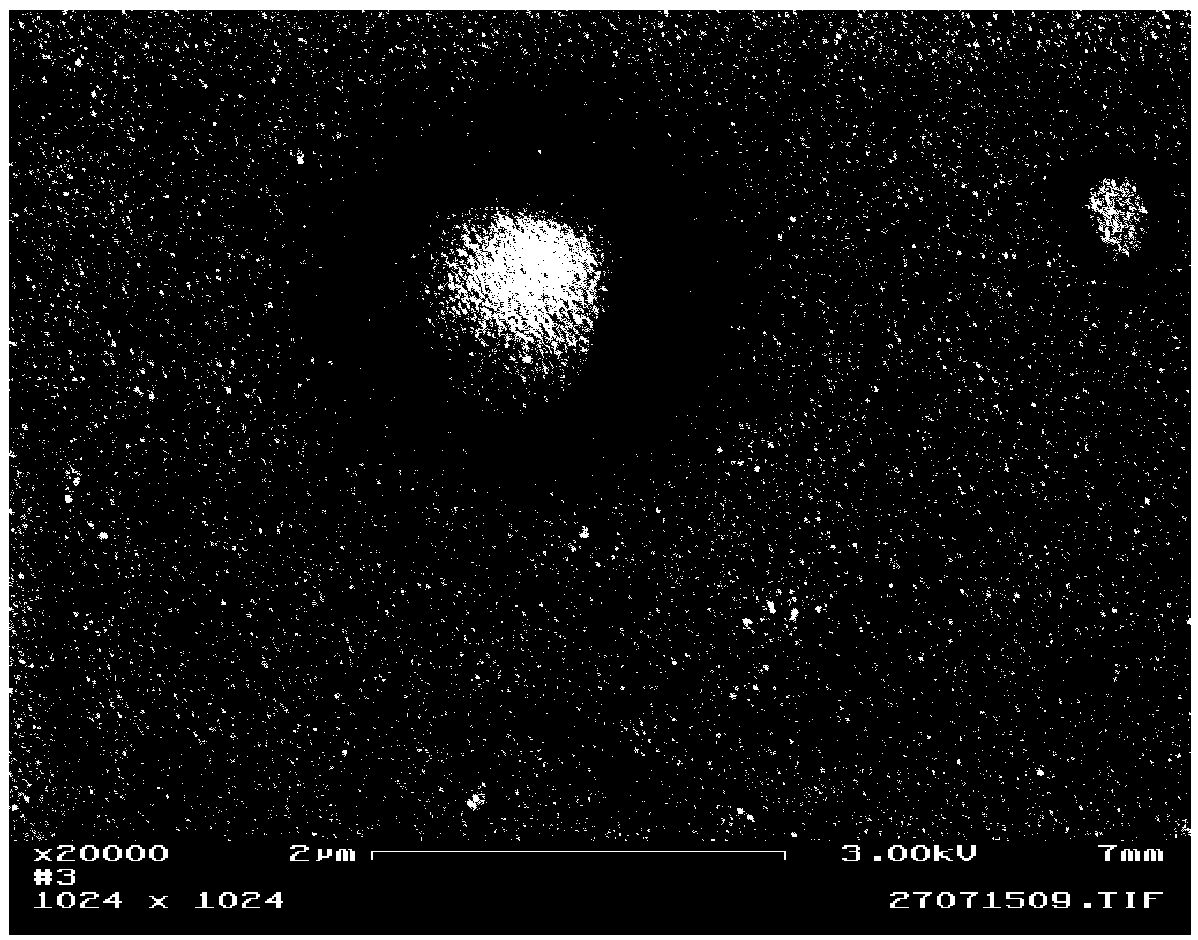
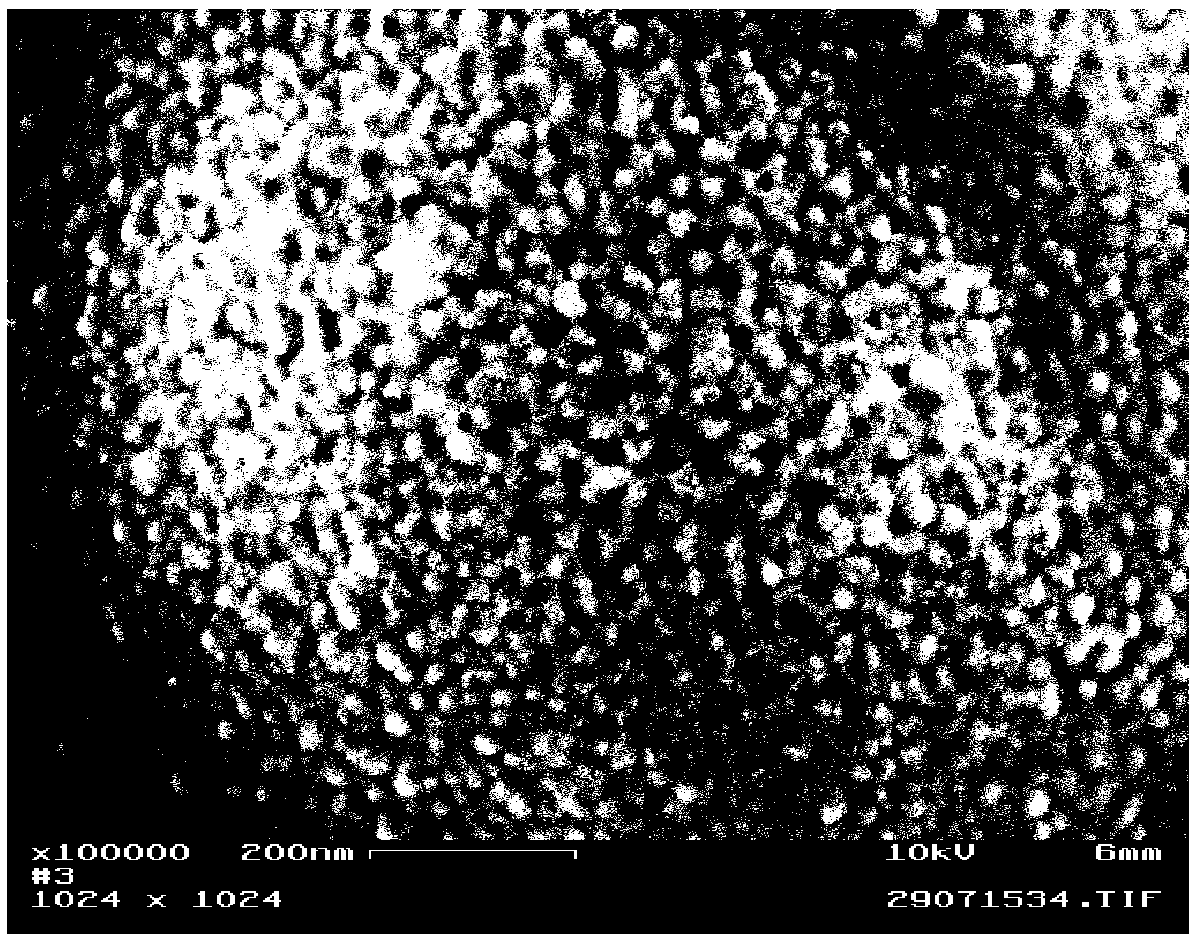
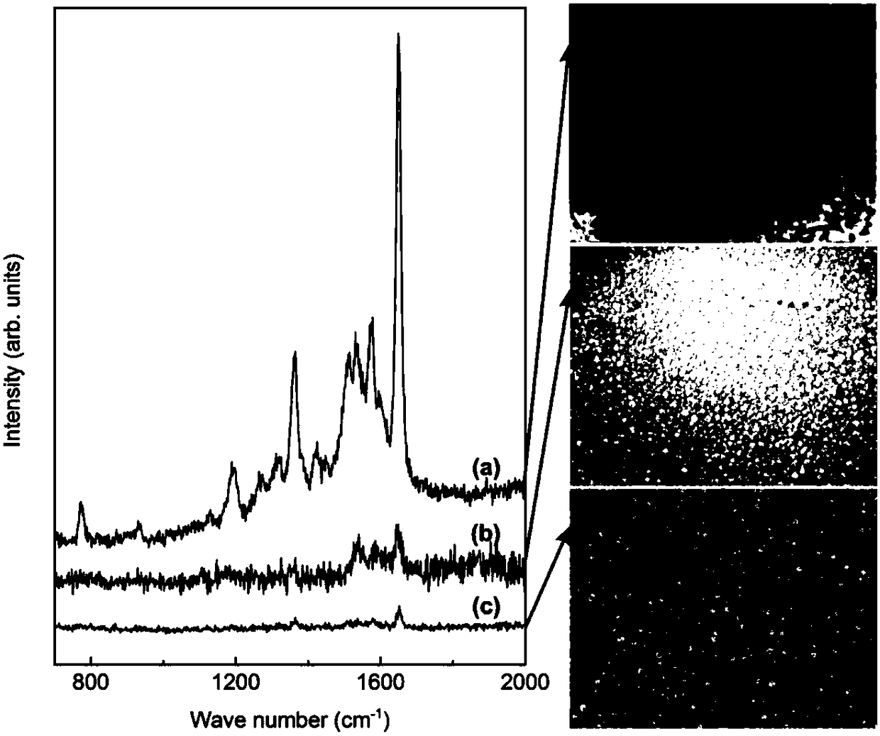
[0051] The present invention prepares Cu on Si substrate by magnetron sputtering 3 N thin film, using SEM to expose the sample to an electron beam, finally forming a nanoporous copper structure, thereby completing the preparation of the SERS substrate. Firstly, the substrate used for depositing samples was ultrasonically cleaned with detergent, acetone, absolute alcohol and deionized water for 15 minutes, and then the substrate was placed on the sample holder of the magnetron sputtering equipment, and the sample holder was parallel to the target surface And the distance is 55mm, when the background pressure in the vacuum chamber is lower than 6×10 -6 At mbar, feed a mixed gas with a flow rate of 40 sccm into the vacuum chamber, and the flow ratio of the mixed gas nitrogen and argon is 20:1; turn on the radio frequency source, preheat for 5 minutes, turn on the radio frequency, and increase the radio frequency power to pre-sputtering Power, the pre-sputtering power is 50W unti...
Embodiment 2
[0053] The present invention prepares Cu on Si substrate by magnetron sputtering 3 N thin film, using SEM to expose the sample to an electron beam, finally forming a nanoporous copper structure, thereby completing the preparation of the SERS substrate. Firstly, the substrate used for depositing samples was ultrasonically cleaned with detergent, acetone, absolute alcohol and deionized water for 15 minutes, and then the substrate was placed on the sample holder of the magnetron sputtering equipment, and the sample holder was parallel to the target surface And the distance is 55mm, when the background pressure in the vacuum chamber is lower than 6×10 -6 At mbar, feed a mixed gas with a flow rate of 30 sccm into the vacuum chamber, and the flow ratio of the mixed gas nitrogen and argon is 10:1; turn on the radio frequency source, preheat for 10 minutes, turn on the radio frequency, and increase the radio frequency power to pre-sputtering Power, the pre-sputtering power is 150W un...
Embodiment 3
[0055] The present invention prepares Cu on Si substrate by magnetron sputtering 3 N thin film, using SEM to expose the sample to an electron beam, finally forming a nanoporous copper structure, thereby completing the preparation of the SERS substrate. Firstly, the substrate used for depositing samples was ultrasonically cleaned with detergent, acetone, absolute alcohol and deionized water for 15 minutes, and then the substrate was placed on the sample holder of the magnetron sputtering equipment, and the sample holder was parallel to the target surface And the distance is 55mm, when the background pressure in the vacuum chamber is lower than 6×10 -6 At mbar, feed a mixed gas with a flow rate of 40 sccm into the vacuum chamber, and the flow ratio of the mixed gas nitrogen and argon is 5:1; turn on the radio frequency source, preheat for 8 minutes, turn on the radio frequency, and increase the radio frequency power to pre-sputtering Power, the pre-sputtering power is 100W unti...
PUM
 Abstract
Description
Claims
Application Information
 - R&D
- Intellectual Property
- Life Sciences
- Materials
- Tech Scout
- Unparalleled Data Quality
- Higher Quality Content
- 60% Fewer Hallucinations
Browse by: Latest US Patents, China's latest patents, Technical Efficacy Thesaurus, Application Domain, Technology Topic, Popular Technical Reports.
© 2025 PatSnap. All rights reserved.Legal|Privacy policy|Modern Slavery Act Transparency Statement|Sitemap|About US| Contact US: help@patsnap.com