

Silicon-based core-shell structure photovoltaic cell and preparation method thereof
A photovoltaic cell and core-shell structure technology, applied in photovoltaic power generation, circuits, electrical components, etc., can solve the problems of many defect states and low photoelectric conversion efficiency, and achieve the effects of reducing defect states, improving photoelectric conversion efficiency, and low temperature
- Summary
- Abstract
- Description
- Claims
- Application Information
AI Technical Summary
Problems solved by technology
Method used
Image

Examples
preparation example Construction
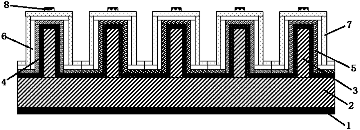
[0024] A method for preparing a silicon-based core-shell structure photovoltaic cell proposed in a specific embodiment of the present invention comprises the following steps:
[0025] (1) preparing a silicon nanowire array on the upper surface of an N-type single crystal silicon wafer, and then soaking in an HF solution to remove the natural silicon oxide on the surface of a single silicon nanowire in the silicon nanowire array;
[0026] (2) Preparation of the first interface modification layer: the upper surface of the N-type single crystal silicon wafer obtained in step (1) is spin-coated with the first mixed solution containing hafnium isobutoxide and P3HT, wherein in the first mixed solution The concentration of hafnium isobutoxide is 0.3-0.5mg / ml, the concentration of P3HT is 1-1.5mg / ml, the rotation speed of spin coating is 5500-6000 rpm, and then the first annealing treatment is performed to form the first Interface modification layer;
[0027] (3) Preparation of the s...
Embodiment 1
[0036] A method for preparing a silicon-based core-shell structure photovoltaic cell, comprising the following steps:
[0037] (1) preparing a silicon nanowire array on the upper surface of an N-type single crystal silicon wafer, and then soaking in an HF solution to remove the natural silicon oxide on the surface of a single silicon nanowire in the silicon nanowire array;
[0038](2) Preparation of the first interface modification layer: the upper surface of the N-type single crystal silicon wafer obtained in step (1) is spin-coated with the first mixed solution containing hafnium isobutoxide and P3HT, wherein in the first mixed solution The concentration of hafnium isobutoxide is 0.4 mg / ml, the concentration of P3HT is 1.2 mg / ml, the rotation speed of spin coating is 5800 rpm, and then the first annealing treatment is performed to form the first interface modification layer;
[0039] (3) Preparation of the second interface modification layer: the upper surface of the N-type ...
Embodiment 2
[0048] A method for preparing a silicon-based core-shell structure photovoltaic cell, comprising the following steps:
[0049] (1) preparing a silicon nanowire array on the upper surface of an N-type single crystal silicon wafer, and then soaking in an HF solution to remove the natural silicon oxide on the surface of a single silicon nanowire in the silicon nanowire array;
[0050] (2) Preparation of the first interface modification layer: the upper surface of the N-type single crystal silicon wafer obtained in step (1) is spin-coated with the first mixed solution containing hafnium isobutoxide and P3HT, wherein in the first mixed solution The concentration of hafnium isobutoxide is 0.5 mg / ml, the concentration of P3HT is 1 mg / ml, the rotation speed of spin coating is 6000 rpm, and then the first annealing treatment is performed to form the first interface modification layer;
[0051] (3) Preparation of the second interface modification layer: the upper surface of the N-type s...
PUM
| Property | Measurement | Unit |
|---|---|---|
| length | aaaaa | aaaaa |
| diameter | aaaaa | aaaaa |
| thickness | aaaaa | aaaaa |
Abstract
Description
Claims
Application Information