A kind of perovskite light-emitting diode based on spraying process and its preparation method

A light-emitting diode and perovskite technology, which is applied in the fields of semiconductor/solid-state device manufacturing, semiconductor devices, electrical components, etc., can solve the problems of limiting the industrialization development of perovskite light-emitting diodes, and the inability to apply large-area devices, and achieve the Small, low roughness, enhanced controllability effect

Active Publication Date: 2019-11-26
UNIV OF ELECTRONICS SCI & TECH OF CHINA
View PDF2 Cites 0 Cited by
  • Summary
  • Abstract
  • Description
  • Claims
  • Application Information

AI Technical Summary

Problems solved by technology

Although the spin-coating method can prepare high-quality uniform films on small-area substrates and obtain high device efficiency, it cannot be applied to the preparation of large-area devices, thus limiting the industrial development of perovskite light-emitting diodes.

Method used


Image

  • A kind of perovskite light-emitting diode based on spraying process and its preparation method
  • A kind of perovskite light-emitting diode based on spraying process and its preparation method
  • A kind of perovskite light-emitting diode based on spraying process and its preparation method

Examples


preparation example Construction

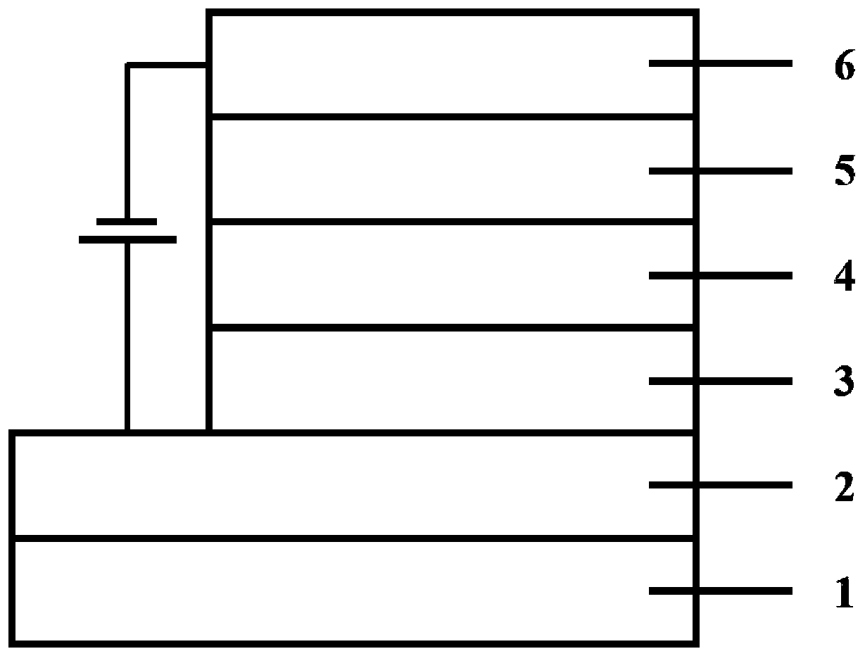
[0027] A method for preparing a perovskite light-emitting diode based on a spraying process, the method comprising the steps of:

[0028] 1. Use ITO glass as the substrate of the substrate, use acetone, deionized water and ethanol solution to ultrasonically clean the substrate, and dry it with dry nitrogen after cleaning.

[0029] 2. Carry out UV pretreatment to the substrate of the substrate produced in step 1.

[0030] 3. Transfer to the glove box, and prepare an anode layer on the substrate treated in step 2. The anode layer is any one or more combinations of ITO, graphene or carbon nanotubes, preferably ITO is the anode.

[0031] 4. In the glove box, use the spraying method to spray a solution of a material with hole transport properties on the anode layer treated in step 3, and then heat the substrate at a temperature of 100-150 °C for 5-15 minutes to prepare a hole transport layer, which has Hole-transport materials can be selected from PEDOT:PSS and traditional polymer...

Embodiment 1

[0046] Spray PEDOT:PSS solution on a transparent conductive substrate, and heat it at 150°C for 10min to prepare a hole transport layer; place the substrate on a low-temperature backplate and cool it down to 5°C, and spray 40wt% dimethyl of PbBr2 and CH3NH3Br Keep the formamide (DMF) solution for 10 minutes; heat the substrate on a hot stage to 80°C for 40 minutes, then spray 2mol / L PCBM chlorobenzene solution; finally spray the alcohol solution of silver nanowires and heat at 100°C 5min, the perovskite light-emitting diode was prepared.

[0047] Its lighting voltage is 3V, and its maximum brightness is 12432cd / m2.

Embodiment 2

[0049] Spray PEDOT:PSS solution on a transparent conductive substrate, and heat at 150°C for 10 minutes to prepare a hole transport layer; place the substrate on a low-temperature backplate and cool it down to -10°C, and spray 20wt% dimethylformamide of PbBr2 and CH3NH3Br Dimethyl formamide (DMF) solution was maintained for 20 minutes; the substrate was placed on a hot stage and heated to 100°C for annealing for 40 minutes, and then sprayed with 2mol / L PCBM chlorobenzene solution; finally, the tungsten wire was heated in a vacuum chamber to evaporate 0.5nm LiF and 100nm Al electrodes were used to fabricate perovskite light-emitting diodes.

[0050] Its lighting voltage is 2.7V, and its maximum brightness is 7632cd / m2.


PUM

PropertyMeasurementUnit
thicknessaaaaaaaaaa
thicknessaaaaaaaaaa
thicknessaaaaaaaaaa

Abstract

The invention discloses a method for preparing a perovskite light-emitting diode based on a spraying process. The method includes the following steps: preparing a substrate for a substrate, and sequentially preparing an anode layer, a hole transport layer, and a perovskite light-emitting layer on the substrate , the electron transport layer and the cathode layer, and finally the obtained substrate is packaged to complete the device preparation, wherein the step of preparing the perovskite light-emitting layer is specifically to place the substrate on a cryogenic plate to cool down, and spray on the hole transport layer Spray the perovskite material solution at one time to obtain the perovskite light-emitting layer, and then place the low-temperature substrate directly on the hot stage for annealing to complete the preparation of the perovskite light-emitting layer. The invention adopts low-temperature one-time spraying to prepare the perovskite light-emitting layer thin film, has low roughness, good crystallinity and small crystal grains, and can improve the brightness and quantum efficiency of the light-emitting diode.

Description

technical field [0001] The invention belongs to the technical field of electroluminescent devices, and in particular relates to a perovskite light-emitting diode based on a spraying process and a preparation method thereof. Background technique [0002] Metal halide perovskite materials can be represented by the chemical formula MAPbX3, where X is Br, I, and Cl. This type of material has excellent optoelectronic properties and can be widely used in optoelectronic devices such as solar cells, photodetectors, and light-emitting diodes. . Perovskite-based light-emitting diodes have the characteristics of high luminous purity, high emission efficiency and low excitation energy, so they may become new light-emitting materials that replace inorganic quantum dots and traditional organic light-emitting materials. [0003] For example, the invention patent with application number 201610635175.9 discloses a double-layer perovskite light-emitting diode and its preparation method; for ...

Claims


Application Information

Patent Timeline
Patent Type & Authority Patents(China)
IPC IPC(8): H01L51/56
CPCH10K71/12H10K71/00
Inventor 于军胜王子君吴梦鸽杨根杰
Owner UNIV OF ELECTRONICS SCI & TECH OF CHINA
Why Eureka
Try Eureka