
Preparing method of phosphorus-doped silicone epitaxial slice for 200 mm Schottky pipe

A technology of epitaxial wafers and phosphorus silicon, which is applied in semiconductor/solid-state device manufacturing, electrical components, circuits, etc., can solve the problems of device yield impact, low growth rate, and increased turn-on voltage, so as to achieve good expansion resistance matching and improve growth Speed, the effect of ensuring production efficiency

Active Publication Date: 2018-08-21
NANJING GUOSHENG ELECTRONICS
View PDF5 Cites 0 Cited by
  • Summary
  • Abstract
  • Description
  • Claims
  • Application Information

AI Technical Summary

Problems solved by technology

[0004] Phosphorus impurities are highly volatile. During the high temperature process of epitaxial production, a large amount of phosphorus impurities will diffuse from the edge and back of the substrate, affecting the accuracy and uniformity of the resistivity of the epitaxial layer.
At present, the measures adopted to solve this problem include growing a layer of SiO2 back-sealing layer on the back and adding a polysilicon back-sealing layer outside the SiO2 back-sealing layer, but the volatilization of impurities in the edge area cannot be avoided; or the method is used during the growth of the entire epitaxial layer At the same time, a small flow of HCL is introduced to remove impurities and achieve better expansion resistance matching. However, the growth rate of this process is low. If the growth rate increases, the expansion resistance will be mismatched, and the lower growth rate affects the silicon epitaxy. Chip production efficiency
At present, the preparation of phosphorus-doped silicon epitaxial wafers for 200mm Schottky tubes mainly uses a monolithic epitaxial furnace, the reaction chamber is small, and the air blowing can not effectively take the impurities out of the reaction chamber, resulting in the volatilized impurities remaining in the stagnant layer on the epitaxial surface , enter the epitaxial layer as doped impurities during epitaxial growth, resulting in excessively high impurity concentration at the interface between the substrate and the epitaxial layer, resulting in widening of the edge transition region, reducing the reliability of the Schottky diode made in the later stage, increasing the turn-on voltage and further Increases energy consumption and affects device yield

Method used

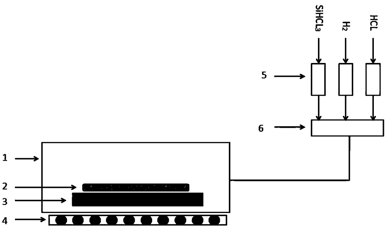
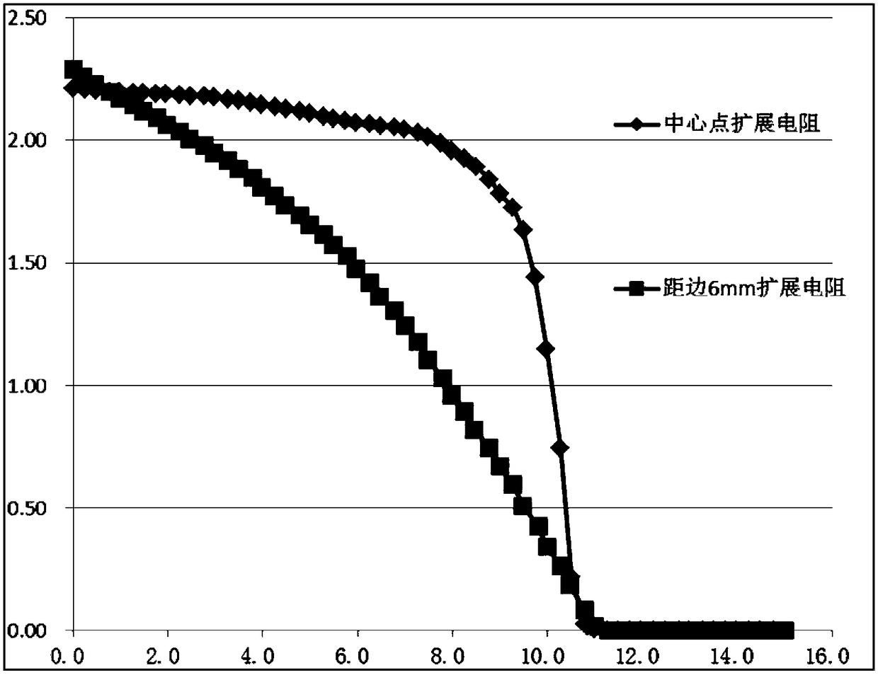
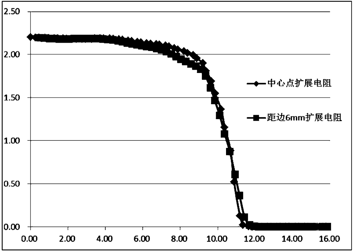

Image

  • Preparing method of phosphorus-doped silicone epitaxial slice for 200 mm Schottky pipe
  • Preparing method of phosphorus-doped silicone epitaxial slice for 200 mm Schottky pipe
  • Preparing method of phosphorus-doped silicone epitaxial slice for 200 mm Schottky pipe

Examples


preparation example Construction

[0026] A kind of preparation method of phosphorus-doped silicon epitaxial wafer for 200mm Schottky tube of the present invention comprises the following steps:

[0027] A. Prepare phosphorus-doped silicon substrate: In order to ensure the requirement of conduction voltage drop, choose phosphorus-doped silicon substrate with a resistivity of 0.0012~0.0015Ωcm. In order to ensure the requirements of STEP lithography machine and the integrity of chip graphics, the substrate Local flatness ≤0.8μm (25mm×25mm), in order to reduce the diffusion of substrate impurities, the back seal layer is silicon dioxide + polysilicon, the thickness of silicon dioxide and polysilicon is

[0028] B. Reaction chamber and substrate cleaning: remove surface impurities and deposited polysilicon layer in epitaxy equipment before epitaxy;

[0029] C. Graphite pedestal treatment: Before epitaxial growth, the pedestal must undergo vapor phase etching treatment again to remove impurities on the surface of ...

Embodiment 1

[0035] A kind of preparation method of phosphorus-doped silicon epitaxial wafer for 200mm Schottky tube of the present invention comprises the following steps:

[0036] A. Prepare phosphorus-doped silicon substrate: choose phosphorus-doped silicon substrate, resistivity 0.0012~0.0015Ωcm, local flatness of substrate ≤0.8μm (25mm×25mm), back seal layer is silicon dioxide + polysilicon, dioxide The thickness of both silicon and polysilicon is

[0037] B. Reaction chamber and substrate cleaning: remove surface impurities and deposited polysilicon layer in epitaxy equipment before epitaxy;

[0038] C. Graphite pedestal treatment: Before epitaxial growth, the pedestal must be reprocessed to remove impurities on the surface of the pedestal and deposited polysilicon layer;

[0039] C. The first layer of encapsulation layer: load a phosphorus-doped silicon substrate, grow a layer of encapsulation layer with a thickness of 0.7 μm on the surface and edge of the substrate, and at the s...

Embodiment 2

[0045] A kind of preparation method of phosphorus-doped silicon epitaxial wafer for 200mm Schottky tube of the present invention comprises the following steps:

[0046] A. Prepare phosphorus-doped silicon substrate: choose phosphorus-doped silicon substrate, resistivity 0.0012~0.0015Ωcm, local flatness of substrate ≤0.8μm (25mm×25mm), back seal layer is silicon dioxide + polysilicon, dioxide The thickness of both silicon and polysilicon is

[0047] B. Reaction chamber and substrate cleaning: remove surface impurities and deposited polysilicon layer in epitaxy equipment before epitaxy;

[0048] C. Graphite pedestal treatment: Before epitaxial growth, the pedestal must undergo vapor phase etching treatment again to remove impurities on the surface of the pedestal and deposited polysilicon layer;

[0049] C. The first layer of encapsulation layer: load a phosphorus-doped silicon substrate, grow a layer of encapsulation layer with a thickness of 0.5 μm on the surface and edge o...


PUM

PropertyMeasurementUnit
thicknessaaaaaaaaaa
thicknessaaaaaaaaaa
thicknessaaaaaaaaaa

Abstract

The invention discloses a preparing method of a phosphorus-doped silicone epitaxial slice for a 200 mm Schottky pipe. The preparing method comprises the following steps of preparing a phosphorus-dopedsilicone substrate, wherein the phosphorus-doped silicone is selected, the electrical resistivity is 0.0012-0.0015 ohm cm, the local flatness of the substrate is smaller than or equal to 0.8 micrometer, a back sealing layer is silicon dioxide and polysilicon, and the thicknesses of both silicon dioxide and polysilicon are shown in the description; preparing a first-layer covering and sealing layer, wherein the covering and sealing layer with the thickness of 0.5-0.8 micrometer is grown on the surface and the edge of the substrate, small-flow HCL is introduced at the same time, and the flow ofHCL is 0.5-1.5 L / min; preparing a second-layer epitaxial layer, wherein HCL is not introduced, doping is introduced, and the epitaxial layer of which the thickness and the electrical resistivity meetrequirements of the 200 mm Schottky pipe is grown. The effective combination of an epitaxial technology not only guarantees matching of the spreading resistance, but also guarantees the production efficiency of the epitaxial slice.

Description

technical field [0001] The invention relates to a silicon epitaxial wafer, a basic semiconductor material, in particular to a method for preparing a phosphorus-doped silicon epitaxial wafer for a 200mm Schottky tube. Background technique [0002] Schottky diodes (SBDs) are majority carrier devices that utilize the contact barrier between metal and semiconductor. Because the height of the Schottky barrier is lower than that of the PN junction, the forward conduction voltage of the SBD is lower than that of the PN junction diode; as a majority carrier device, the reverse recovery time will not be affected by the lifetime of the minority carriers, it only depends on Due to the charging and discharging time of the Schottky barrier capacitor, the switching speed is fast and the switching loss is small. Based on the above characteristics, Schottky diodes are used as rectification and freewheeling elements in high-frequency rectification, protection circuits and switching circuits...

Claims


Application Information

Patent Timeline
Patent Type & Authority Applications(China)
IPC IPC(8): H01L21/329
CPCH01L29/6609
Inventor 尤晓杰邓雪华刘勇潘文宾
Owner NANJING GUOSHENG ELECTRONICS
Learn More