

Piezoelectric optoelectronic material for degradation of organic pollutants and degradation method thereof
A technology of organic pollutants and optoelectronics, applied in the field of pollutant treatment, can solve the problem that the ability to degrade pollutants cannot meet the requirements, and achieve the effects of stable performance, strong adsorption capacity and efficient removal
- Summary
- Abstract
- Description
- Claims
- Application Information
AI Technical Summary
Problems solved by technology
Method used
Image

Examples
preparation example Construction
[0041] Two-dimensional KNbO 3 Concrete preparation examples of nanosheets:
[0042] (1) Weigh 1.403g KOH and 0.35g Nb 2 o 5 , successively added to a 100mL beaker containing 25mL of ethylene glycol;
[0043] (2) Place the beaker containing the above mixed solution on a magnetic stirrer (stirring speed: 500rpm) and stir for 45 minutes to fully disperse;
[0044] (3) Put the above mixed solution into a polytetrafluoroethylene lining, and heat at 200° C. for 12 hours.
[0045] (4) After cooling to room temperature, wash with distilled water and ethanol for more than three times, and dry to obtain a white product.
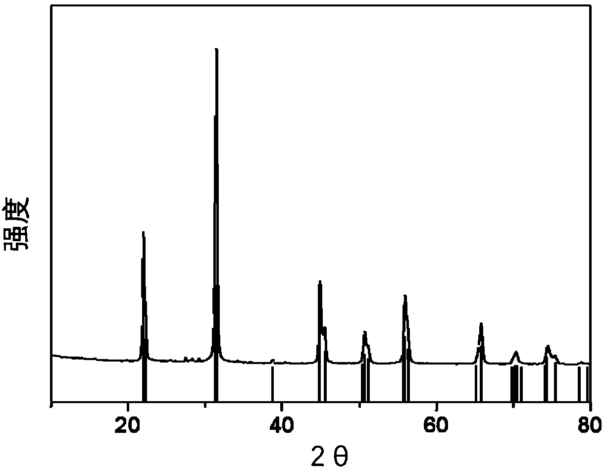
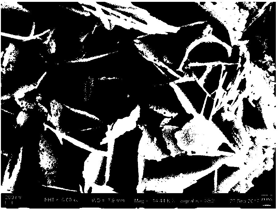
[0046] (5) Grind the above white product with an agate mortar for 5 minutes, place the obtained powder in a muffle furnace, and then calcinate it at 900°C for 2 hours to obtain a two-dimensional KNbO with a thickness of 50nm and a length of 300nm 3 Nanosheets.
[0047] see figure 1 , figure 2 , KNbO prepared by the present invention 3 Nanosheets, under SEM ob...
PUM
| Property | Measurement | Unit |
|---|---|---|
| Length | aaaaa | aaaaa |
| Thickness | aaaaa | aaaaa |
| Length | aaaaa | aaaaa |
Abstract
Description
Claims
Application Information