Silicon-based avalanche photoelectric detector array and manufacturing method thereof

A detector array, avalanche photoelectric technology, applied in the direction of electric solid devices, circuits, electrical components, etc., can solve the problems of APD array system performance degradation, affecting the responsivity of the imaging system, etc., to reduce costs, prevent lateral photoelectric crosstalk, The effect of strong practicality

Active Publication Date: 2018-09-25
INST OF SEMICONDUCTORS - CHINESE ACAD OF SCI
View PDF11 Cites 16 Cited by
  • Summary
  • Abstract
  • Description
  • Claims
  • Application Information

AI Technical Summary

Problems solved by technology

[0003] On the other hand, in the APD array, the APD units are arranged in an array, and the distance between adjacent APD units is not enough to suppress the photoelectric crosstalk between these adjacent units. Such photoelectric crosstalk will reduce the performance of the APD array system and affect the entire system. Responsivity, linearity and other characteristics of the imaging system
Therefore, in order to eliminate the influence of the above-mentioned photoelectric crosstalk, those skilled in the art have carried out various practices, and the results of these practices are reflected in the documents of the prior art such as U.S. Patent No. Barrier structures such as insulating trenches and mirrors are set to prevent photons (secondary photons) from traveling to adjacent APD units through specific optical effects. Although these means reduce the photoelectric crosstalk between adjacent units to a certain extent, because the two The formation of secondary photons is mainly due to the fact that when the APD is working, after the incident photons are absorbed by the absorbing layer, ionization collisions occur in the multiplication layer to realize the multiplication of photo-generated carriers, and each carrier will be released under the reverse bias of the PN junction. A secondary photon is emitted with a certain probability, and the secondary photon will enter the adjacent APD unit isotropically from any possible channel, and these blocking structures cannot completely prevent the secondary photon from entering the adjacent unit, so how to effectively and completely prevent the APD array from Optical and electrical crosstalk between adjacent APD units is still an issue currently facing the art

Method used


Image

  • Silicon-based avalanche photoelectric detector array and manufacturing method thereof
  • Silicon-based avalanche photoelectric detector array and manufacturing method thereof
  • Silicon-based avalanche photoelectric detector array and manufacturing method thereof

Examples


Embodiment Construction

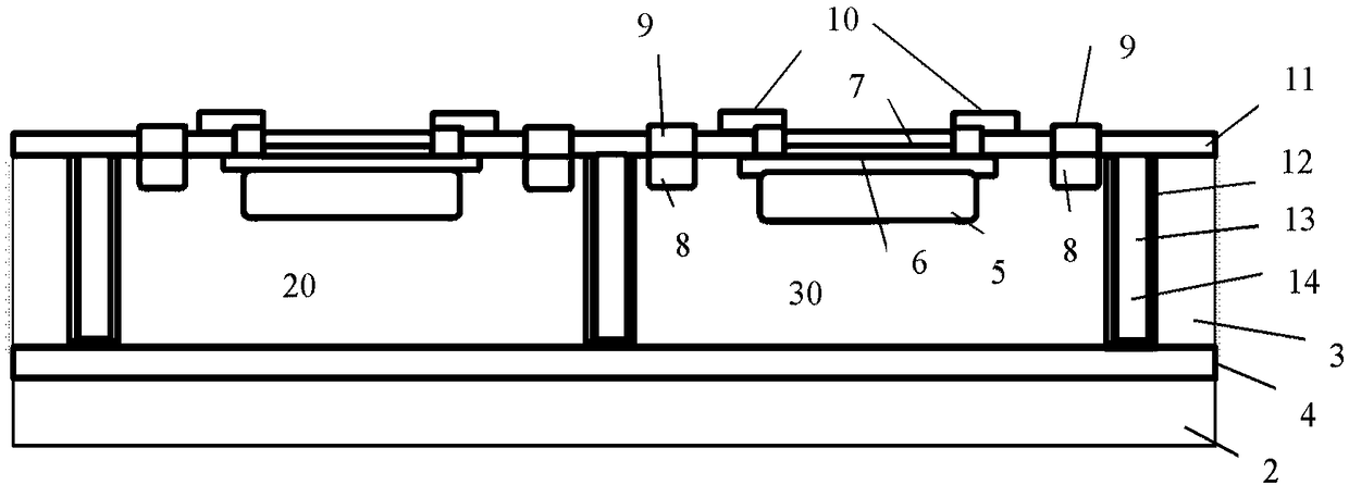
[0036] To solve the aforementioned technical problems, there are two key points: one is the deep trench between the APD units, the high reflectivity multilayer dielectric film set on the side wall and bottom of the deep trench, and the multilayer dielectric film formed by the multilayer dielectric film. The high anti-insulation deep trench structure (also called "trench structure"), such as the insulating medium filled in the trench space, can block the lateral transmission path of photoelectric crosstalk, so as to realize the effective suppression of the lateral transmission of photoelectric crosstalk; the second is based on Bonded Epitaxial Si / SiO 2 SiO in / Si material structure 2 The APD array structure of the / Si composite substrate can effectively suppress the photoelectric crosstalk, thereby realizing photodetection with low crosstalk and high responsivity.

[0037] To realize high-efficiency photodetectors, the present invention provides an APD array comprising a highl...


PUM


Abstract

The invention provides a silicon-based avalanche photoelectric detector array and a manufacturing method thereof. According to a device main structure of the silicon-based avalanche photoelectric detector array, a wafer structure with an epitaxial Si layer is formed on a SiO2 / Si composite substrate, the wafer structure is an epitaxial Si / SiO2 / Si material structure forming by a bonding technology,the silicon-based avalanche photoelectric detector array based on the wafer structure comprises the SiO2 / Si composite substrate, avalanche photoelectric detector (APD) units arranged on the SiO2 / Si composite substrate in an array, and a trench structure formed surrounding the APD units, and the sidewall and bottom of the trench structure are deposited with a high-reflection dielectric film. Thus,the high-reflection dielectric film of the trench structure blocks lateral light crosstalk from adjacent APD units, a SiO2 bonding interface based on the SiO2 / Si composite substrate blocks secondary photons from entering the adjacent APDs via the substrate, the crosstalk path among the APD units is cut off effectively, the integral performance of the APD array is improved, the APD array of a largearea array can be integrated compactly, and the batch production performance is improved.

Description

technical field [0001] The invention relates to the technical field of silicon-based avalanche photodetectors, in particular to a method for transferring epitaxial Si layers to SiO based on bonding technology. 2 An avalanche photodetector array with eliminated photoelectric crosstalk on a Si composite substrate and a fabrication method thereof. Background technique [0002] Avalanche Photodiode (APD) has been widely used in optical fiber communication, laser ranging, Laser fuze, spectral measurement, remote sensing measurement, medical image diagnosis, environmental monitoring and military reconnaissance, etc., are laser intensity directional ranging (Laser Intensity Direction and Ranging, LIDAR, laser radar) system, 3D laser scanning system, nuclear medicine Core devices in high-tech practices such as imaging systems and high-energy physics systems. In contrast, the development of infrared focal plane technology is relatively mature, and large-array infrared focal plane d...

Claims


Application Information

Patent Timeline
Patent Type & Authority Applications(China)
IPC IPC(8): H01L27/146
CPCH01L27/14623H01L27/1463H01L27/14643H01L27/14685
Inventor 郑婉华彭红玲
Owner INST OF SEMICONDUCTORS - CHINESE ACAD OF SCI
Why Eureka
Try Eureka