Manufacturing method of double-junction thin film solar cell module and cell module thereof

A technology of solar cells and manufacturing methods, which is applied to electrical components, circuits, photovoltaic power generation, etc., can solve the problems of inability to achieve battery flexibility and large overall thickness of the battery, and achieve improved conversion efficiency and product yield, improved crystal quality, and improved efficiency effect

Inactive Publication Date: 2018-10-16
DONGTAI HI TECH EQUIP TECH (BEIJING) CO LTD
View PDF0 Cites 0 Cited by
  • Summary
  • Abstract
  • Description
  • Claims
  • Application Information

AI Technical Summary

Problems solved by technology

[0007] In addition, the thickness of the absorption layer of the double-junction GaAs and GaInP is relatively large, resulting in the overall thickness of the cell being greater than 10 μm
However, the thickness of flexible thin-film batteries is generally required to be between 1-10 μm, and this type of double-junction battery cannot achieve battery flexibility.

Method used


Image

  • Manufacturing method of double-junction thin film solar cell module and cell module thereof
  • Manufacturing method of double-junction thin film solar cell module and cell module thereof
  • Manufacturing method of double-junction thin film solar cell module and cell module thereof

Examples


Embodiment 1

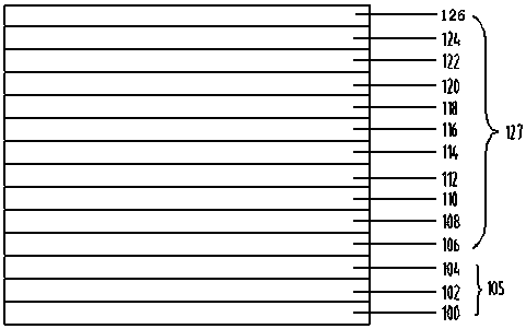
[0090]In step one, a GaAs buffer layer 102 and a sacrificial layer 104 are sequentially grown on the GaAs substrate 100 .

[0091] The double-junction battery structure is epitaxially grown on the GaAs substrate by MOCVD and other epitaxial equipment, and the pressure of the epitaxial reaction chamber is 76torr.

[0092] A. Firstly, the temperature of the GaAs substrate 100 is raised to 750° C. for 3 minutes to clean the GaAs substrate and form a step plane for epitaxial growth. Then lower the temperature to 600°C to start growing the cell epitaxial structure;

[0093] B. growing a 200nm GaAs buffer layer 102 on the surface of the N-type GaAs substrate 100;

[0094] C. A 30 nm AlAs sacrificial layer 104 is grown on the surface of the buffer layer 102 .

[0095] Step 2, forming an inverted growth GaAs top cell on the surface of the sacrificial layer 104

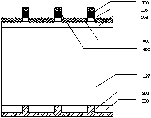
[0096] A. On the AlAs sacrificial layer 104, grow a 15nm P+ type GaAs front contact layer 106 with a doping concentration...

Embodiment 2

[0128] In step one, a GaAs buffer layer 102 and a sacrificial layer 104 are sequentially grown on the GaAs substrate 100 .

[0129] The double-junction battery structure is epitaxially grown on the GaAs substrate by MOCVD and other epitaxial equipment, and the pressure of the epitaxial reaction chamber is 100torr.

[0130]A. Firstly, the temperature of the GaAs substrate 100 is raised to 750° C. for 4 minutes to clean the GaAs substrate and form a step plane for epitaxial growth. Then lower the temperature to 650°C to start growing the cell epitaxial structure;

[0131] B. growing a 50nm GaAs buffer layer 102 on the surface of the GaAs substrate 100;

[0132] C. A 20 nm AlAs sacrificial layer 104 is grown on the surface of the buffer layer 102 .

[0133] Step 2, forming an inverted growth GaAs top cell on the surface of the sacrificial layer 104

[0134] A. On the AlAs sacrificial layer 104, grow a 10nm P+ type GaAs front contact layer 106 with a doping concentration of 2E ...


PUM


Abstract

The invention discloses a method of double-junction thin film solar cell module and cell module thereof. The cell module is formed by connecting a plurality of battery units, each battery unit comprises a bottom battery and a top battery, wherein a patterned insulating layer and a back metal electrode layer electrically connected with the bottom battery are arranged on the bottom battery, and a patterned front metal electrode layer is arranged on the top battery, the bottom battery is a polycrystalline Ge bottom battery, and the top battery is a GaAs top cell, the layers of the bottom cells and the layers of the top cells are inverted and grown in an epitaxial manner, a tunnel junction N-type region and a tunnel junction P-type region are sequentially grown between the GaAs top battery andthe polycrystalline Ge bottom battery; an antireflection layer is formed on the front metal electrode layer and the top battery which is not covered by the front metal electrode layer. According to the manufacturing method of double-junction thin film solar cell module and cell module thereof, by adopting the inverted growth mode, the crystal quality is improved, and by adopting the method of one-time growth to complete the battery structure, the process can be simplified, and the yield of the product can be improved, in addition, by using Ge as the bottom battery, there is no need for a complicated battery structure and current transmission is improved.

Description

technical field [0001] The invention relates to the field of III-V double-junction thin-film batteries, and more specifically, relates to a method for manufacturing a double-junction thin-film solar battery module and the battery module. Background technique [0002] In 1954, it was first discovered that GaAs material has photovoltaic effect in the world. In the 1960s, Gobat et al. developed the first zinc-doped GaAs solar cell, with a conversion rate of only 9% to 10%, far lower than the theoretical value of 27%. The earliest monocrystalline GaAs cells were basically the same as the current monocrystalline silicon, but as a direct bandgap semiconductor, the thickness of the absorbing layer only needs to be a few microns, and crystalline GaAs is undoubtedly a huge waste. [0003] In the 1970s, research institutes represented by IBM and the Ioffe Institute of Technical Physics of the former Soviet Union adopted LPE (liquid phase epitaxy) technology to introduce a GaAlAs heter...

Claims


Application Information

Patent Timeline
Patent Type & Authority Applications(China)
IPC IPC(8): H01L31/18H01L31/0687
CPCH01L31/0687H01L31/18Y02E10/544Y02P70/50
Inventor 顾世海
Owner DONGTAI HI TECH EQUIP TECH (BEIJING) CO LTD
Why Eureka
Try Eureka