

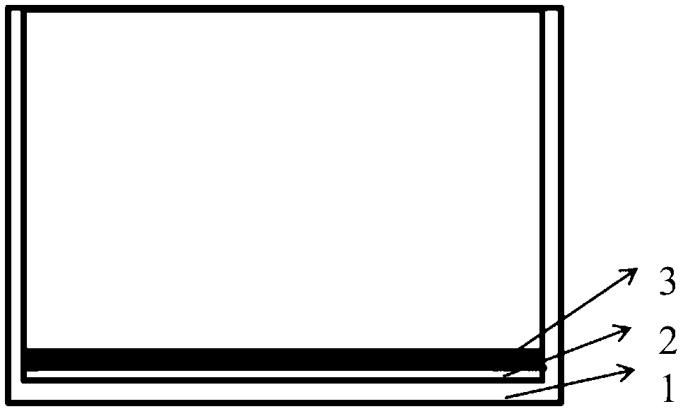
Pseudo-single crystal silicon ingot casting crucible with aluminum oxide thin film used as barrier layer
A quasi-single crystal silicon and barrier layer technology, applied in the directions of single crystal growth, single crystal growth, coating, etc., can solve the problems of limited effect of the width of the red zone at the bottom of the silicon ingot, increase the cost of the ingot, high production cost, etc. Achieve the effect of low red zone width, improved utilization rate and high minority carrier lifetime
- Summary
- Abstract
- Description
- Claims
- Application Information
AI Technical Summary
Problems solved by technology
Method used
Image

Examples
Embodiment 1
[0030] (1) Provide a crucible with an inner diameter of 175*175mm and a height of 190mm, and coat a silicon nitride coating on the inner bottom of the crucible, and the thickness of the silicon nitride coating is 40 μm;
[0031] (2) On a solar-grade monocrystalline silicon wafer with a thickness of 0.2mm and a specification of 170*170mm;
[0032] (3) Deposit Al at 150°C by ALD method on the solar-grade monocrystalline silicon wafer 2 o 3 film, and paste it on the bottom of the crucible through high-purity silica sol;
[0033] The process parameters of the ALD method are: the deposition temperature is 150°C, the nitrogen pressure is 0.15torr, the TMA pulse time is 0.02s; the water vapor pulse time is 0.015s; the deposition cycle is 125 times;
[0034] The Al 2 o 3 The thickness of the film is 15nm;
[0035] (4) Then set a seed crystal on the barrier layer at the bottom of the crucible with a barrier layer, and then set silicon material on the seed crystal, then heat, melt,...
Embodiment 2
[0039] (1) Provide a crucible with an inner diameter of 175*175mm and a height of 190mm, and coat a silicon nitride coating on the inner bottom of the crucible, and the thickness of the silicon nitride coating is 80 μm;
[0040] (2) On a solar-grade monocrystalline silicon wafer with a thickness of 0.2mm and a specification of 170*170mm;
[0041] (3) Deposit Al on the solar-grade monocrystalline silicon wafer by ALD at 200°C 2 o 3 film, and paste it on the bottom of the crucible through high-purity silica sol;
[0042] The process parameters of the ALD method are: the deposition temperature is 200°C, the nitrogen pressure is 0.2torr, the TMA pulse time is 0.025s; the water vapor pulse time is 0.02s; the deposition cycle is 209 times;
[0043] The Al 2 o 3 The thickness of the film is 25nm;
[0044] (4) Then set the seed crystal on the barrier layer at the bottom of the crucible with barrier layer, and then set the silicon material on the seed crystal, after heating, melti...
Embodiment 3
[0047] (1) Provide a crucible with an inner diameter of 175*175mm and a height of 190mm, and coat a silicon nitride coating on the inner bottom of the crucible, and the thickness of the silicon nitride coating is 40 μm;
[0048] (2) On a solar-grade monocrystalline silicon wafer with a thickness of 0.2mm and a specification of 170*170mm;
[0049] (3) Deposit Al on the solar-grade monocrystalline silicon wafer by ALD at 200°C 2 o 3 film, and paste it on the bottom of the crucible through high-purity silica sol;
[0050] The process parameters of the ALD method are: the deposition temperature is 200°C, the nitrogen pressure is 0.15torr, the TMA pulse time is 0.02s; the water vapor pulse time is 0.015s; the deposition cycle is 167 times;
[0051] The Al 2 o 3 The thickness of the film is 20nm;
[0052] (4) Then set a seed crystal on the barrier layer at the bottom of the crucible with a barrier layer, and then set silicon material on the seed crystal, then heat, melt, grow c...
PUM
| Property | Measurement | Unit |
|---|---|---|
| The inside diameter of | aaaaa | aaaaa |
| Height | aaaaa | aaaaa |
| Thickness | aaaaa | aaaaa |
Abstract
Description
Claims
Application Information