Oxide film transistor and manufacturing method thereof

An oxide thin film and transistor technology, applied in the field of microelectronics, can solve problems such as limited capacitive coupling effect, inconformity with low energy consumption, portable applications, etc., and achieve the effects of simplifying process complexity, reducing process cost, and reducing operating voltage

Active Publication Date: 2018-11-13
NINGBO INST OF MATERIALS TECH & ENG CHINESE ACADEMY OF SCI
View PDF1 Cites 16 Cited by
  • Summary
  • Abstract
  • Description
  • Claims
  • Application Information

AI Technical Summary

Problems solved by technology

However, oxide TFT usually uses the traditional dielectric oxide film as the gate dielectric, and its capacitive coupling effect is limited. Therefore, a high operating voltage is usually required to obtain high mobility and current switching ratio, which does not meet the requirements of low energy consumption and portable applications. Require

Method used


Image

  • Oxide film transistor and manufacturing method thereof
  • Oxide film transistor and manufacturing method thereof
  • Oxide film transistor and manufacturing method thereof

Examples


example

[0060] Example: Chitosan thin film is deposited on ITO conductive glass substrate, which has a strong electric double layer control effect. The thin film is used as gate dielectric to make InZnO thin film transistor, and the threshold voltage of the device is 0.6V. After applying a bias voltage with a pulse height of 2V and a pulse width of 5s on the gate electrode, the threshold voltage of the device drifted negatively to 0.3V.

[0061] Principle of manufacturing method

[0062] According to the above concept of the present invention, a method for manufacturing an oxide thin film transistor is provided, comprising the steps of: using an oxide semiconductor thin film as a channel of the transistor, which has electronic conductivity; using a solid electrolyte with proton conductivity as a gate dielectric, Therefore, the manufactured device is an n-type oxide thin film transistor; voltage pulses are applied to the gate electrode to realize optimization of device performance and ...

Embodiment 1

[0082] Example 1: Oxide thin film transistor (bottom gate type)

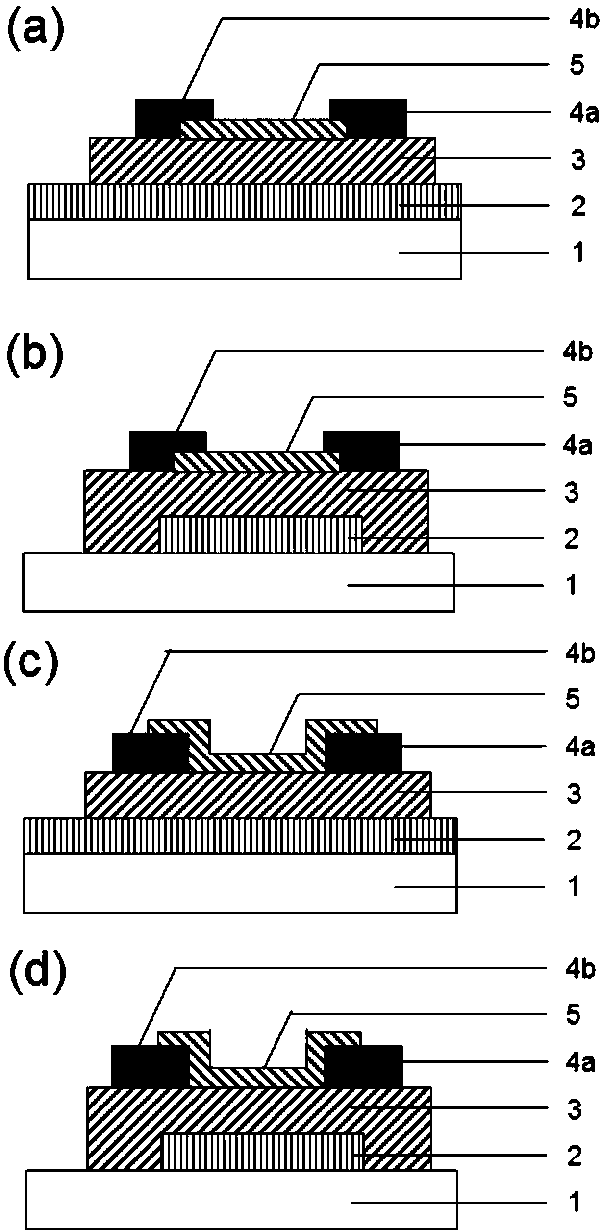
[0083] figure 1 (a)-1(d) respectively show four structures of bottom gate oxide TFTs according to an embodiment of the present invention, these four structures are respectively: bottom gate top contact type, see figure 1 (a) and 1(b), bottom gate bottom contact type, see figure 1 (c) and 1(d).

[0084] As shown in the figure, each bottom-gate oxide TFTs includes: an insulating substrate 1, a bottom-gate electrode 2, a gate dielectric layer 3, a drain 4a, a source 4b, and a channel 5, wherein one of the gate dielectric layers 3 One side is the bottom gate electrode 2, and the other side is the drain 4a, the source 4b, and the channel 5 between them.

[0085] The above-mentioned layered structure of the bottom-gate oxide TFTs is similar to that in the prior art, and will not be repeated here. It should be noted that the gate dielectric layer 3 is a solid electrolyte with proton conductivity. As mentioned abov...

Embodiment 2

[0086] Example 2: Oxide thin film transistor (top gate type)

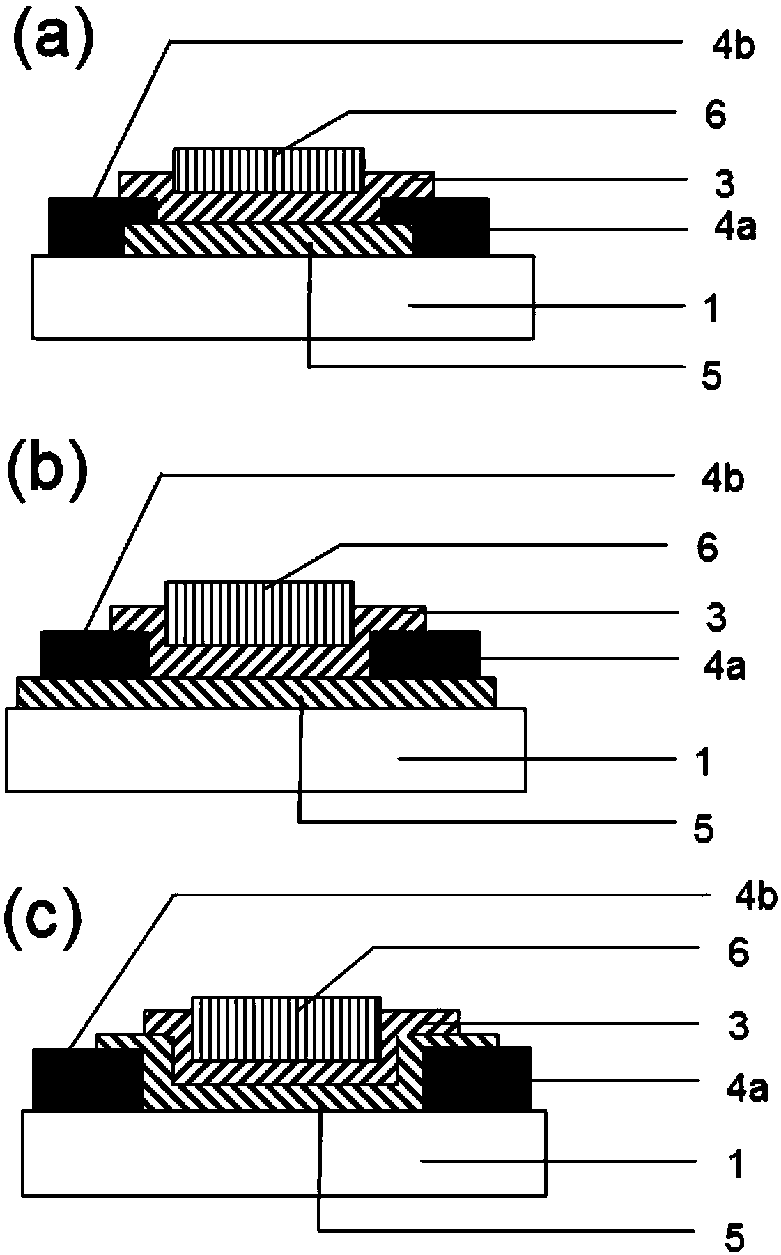
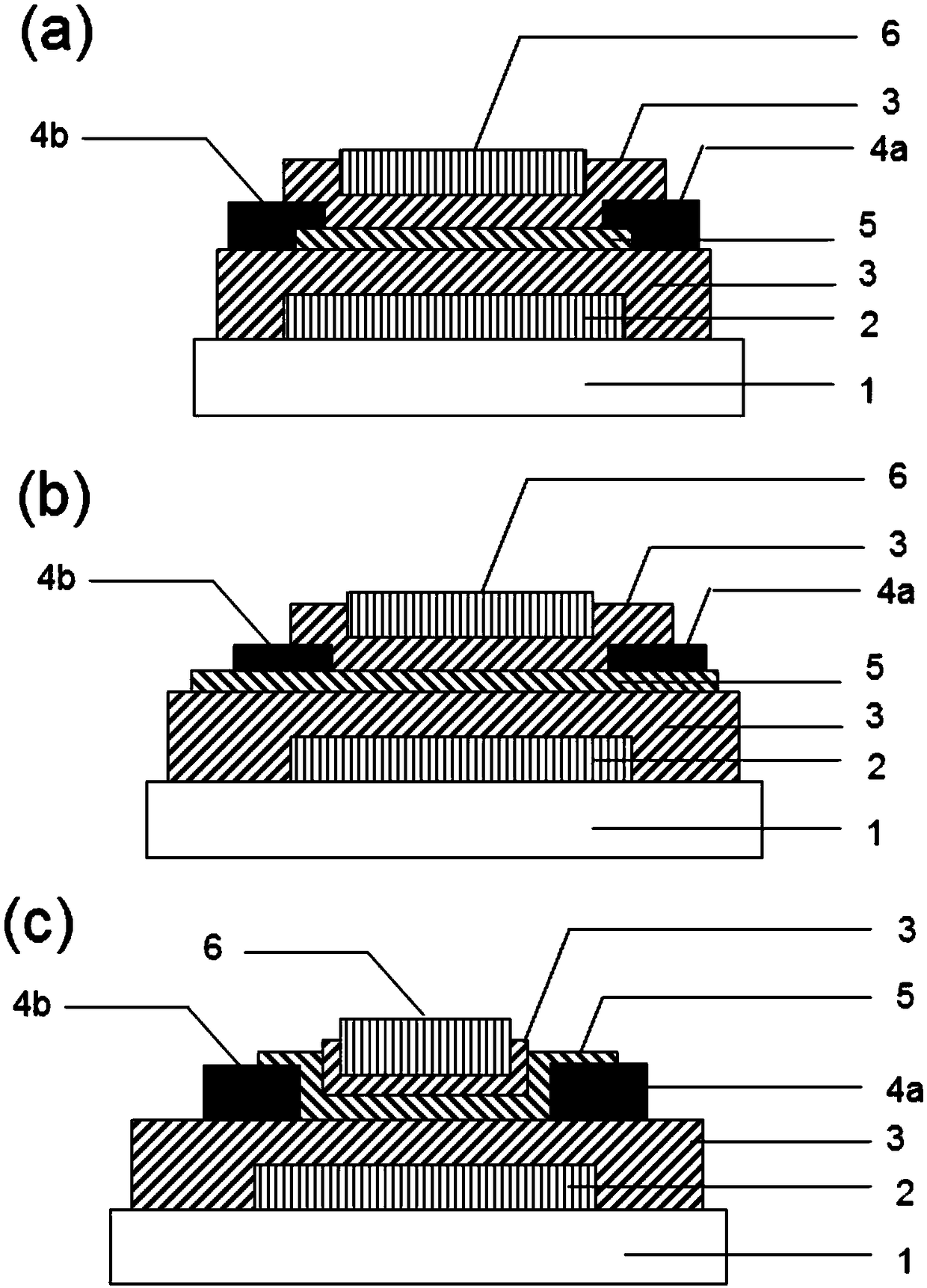
[0087] figure 2 (a)-2(c) respectively show three structures of top gate oxide TFTs according to another embodiment of the present invention, these three structures are respectively: top gate top contact type, see figure 2 (a) and 2(b), bottom gate bottom contact type, see figure 2 (c).

[0088] Similar to the previous embodiment, each top-gate oxide TFTs includes: an insulating substrate 1, a top-gate electrode 6, a gate dielectric layer 3, a drain 4a, a source 4b, and a channel 5, wherein the gate dielectric layer 3 One side is the top gate electrode 6, and the other side is the drain 4a, the source 4b, and the channel 5 between them.

[0089] The layered structure of the above-mentioned top-gate oxide TFTs is similar to that in the prior art, and will not be repeated here. It should be noted that the gate dielectric layer 3 is a solid electrolyte with proton conductivity. As mentioned above, the solid ele...


PUM


Abstract

The invention discloses an oxide film transistor comprising an insulation substrate, a gate medium layer, a grid electrode arranged on one side of the gate medium layer, a source electrode and a drainelectrode arranged on the other side of the gate medium layer, and a channel layer between the source electrode and the drain electrode; the gate medium is a solid electrolyte with proton conductivecharacteristics, and a grid electrode bias pulse can be applied to regulate a transistor threshold voltage; the oxide film transistor can be either of the following structure types: a bottom gate topcontact type, a bottom gate bottom contact type, a top gate top contact type, a top gate bottom contact type, and a bottom gate and top gate combined type. The oxide film transistor can effectively reduce the work voltage; the grid electrode bias voltage can be applied to regulate the device threshold voltage according to needs, thus simplifying the process complexity, and reducing the process cost.

Description

technical field [0001] The invention relates to the technical field of microelectronics, in particular to a structure and a manufacturing method of an oxide thin film transistor with low operating voltage. Background technique [0002] Thin-film transistors (TFTs) are an important class of semiconductor devices, which have great application value in new-generation electronic products, including flexible wearable devices, new-generation flat panel displays, portable sensing, bioelectronics devices etc. Therefore, thin film transistors have become an indispensable part of contemporary microelectronics technology. [0003] In 1964, Klasens et al reported the first oxide TFT, they used tin oxide (SnO2) as the channel layer of the device. In 2003, after Nomura et al. successively published the relevant research results of indium gallium zinc oxide (InGaZnO) TFT in Science and Nature, the related research entered a period of rapid development. Wide-bandgap oxide semiconductors ...

Claims


Application Information

Patent Timeline
Patent Type & Authority Applications(China)
IPC IPC(8): H01L29/786H01L29/51H01L21/34
CPCH01L29/51H01L29/66969H01L29/7869
Inventor 竺立强刘锐肖惠付杨明
Owner NINGBO INST OF MATERIALS TECH & ENG CHINESE ACADEMY OF SCI
Why Eureka
Try Eureka