

A kind of stress control catalyst thin film electrode and its preparation method and application
A thin-film electrode and stress control technology, which is applied in the direction of electrodes, electrolytic components, electrolytic process, etc., can solve the problems of large-scale commercialization of technology, and achieve the effect of low cost and simple preparation method
- Summary
- Abstract
- Description
- Claims
- Application Information
AI Technical Summary
Problems solved by technology
Method used
Image

Examples
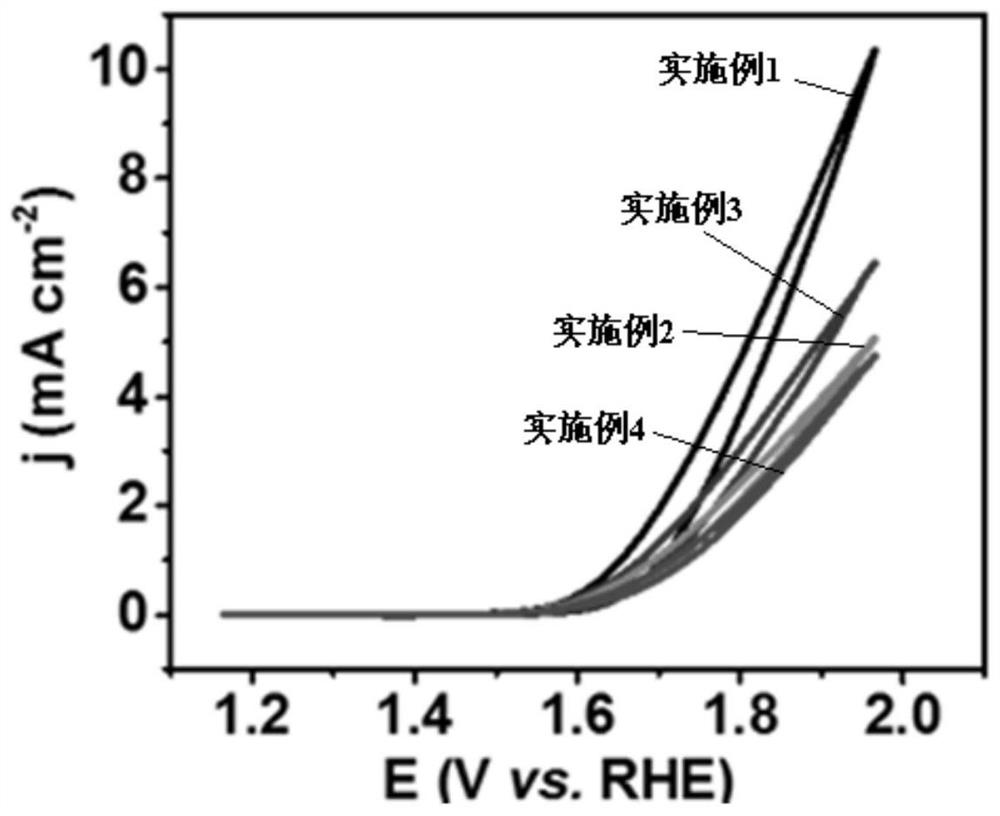
Embodiment 1
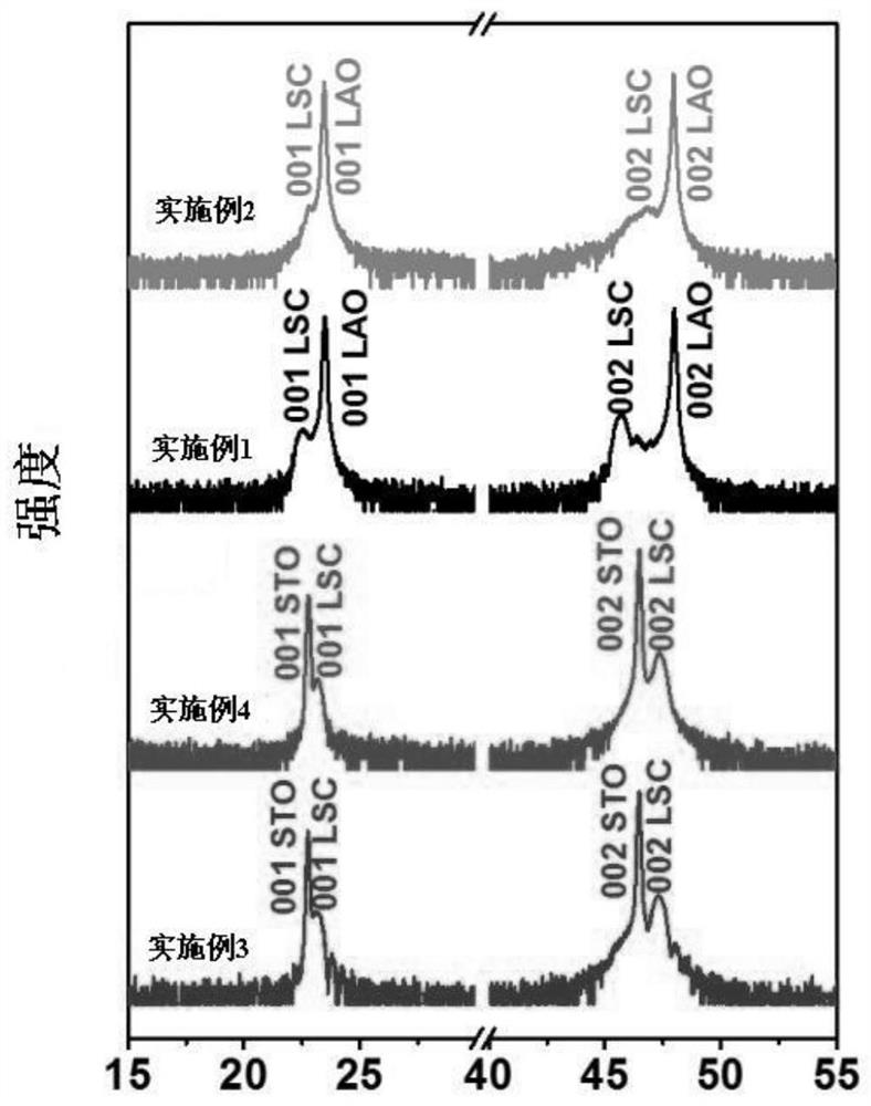
[0028] The preparation of a stress-regulating catalyst thin film electrode in this embodiment, the specific preparation steps are as follows:
[0029] (1) Strontium carbonate, lanthanum oxide and cobalt oxide are pressed by La 0.7 Sr 0.3 CoO 3 The stoichiometric ratio was mixed evenly by high-speed ball milling for 12 hours, and sintered in a muffle furnace at 1200°C to obtain La 0.7 Sr 0.3 CoO 3 powder, which is then pressed into a target in a mold;
[0030] (2) in LaAlO 3 (001) 10nm Au conductive network deposited by ion sputtering on a single crystal substrate (LAO);
[0031] (3) Using the target obtained in step (1) on the substrate on which the Au conductive network was deposited in step (2) by pulsed laser sputtering deposition (PLD) to obtain La with stress difference from the substrate 0.7 Sr 0.3 CoO 3 Thin film; PLD parameters are: substrate temperature 600°C, oxygen pressure 200Pa, laser energy 300mj, laser frequency 5Hz, deposition time 3min, laser frequenc...
Embodiment 2
[0034] The preparation of a stress-regulating catalyst thin film electrode in this embodiment, the specific preparation steps are as follows:
[0035] (1) Strontium carbonate, lanthanum oxide and cobalt oxide are pressed by La 0.7 Sr 0.3 CoO 3 The stoichiometric ratio was mixed evenly by high-speed ball milling for 12 hours, and sintered in a muffle furnace at 1200°C to obtain La 0.7 Sr 0.3 CoO 3 powder, which is then pressed into a target in a mold;
[0036] (2) in LaAlO 3 (001) 10nm Au conductive network deposited by ion sputtering on a single crystal substrate (LAO);
[0037] (3) Using the target obtained in step (1) on the substrate on which the Au conductive network was deposited in step (2) by pulsed laser sputtering deposition (PLD) to obtain La with stress difference from the substrate 0.7 Sr 0.3 CoO 3 Thin film; PLD parameters are: substrate temperature 600°C, oxygen pressure 200Pa, laser energy 300mj, laser frequency 5Hz, deposition time 6min, laser frequenc...
Embodiment 3
[0040]The preparation of a stress-regulating catalyst thin film electrode in this embodiment, the specific preparation steps are as follows:
[0041] (1) Strontium carbonate, lanthanum oxide and cobalt oxide are pressed by La 0.7 Sr 0.3 CoO 3 The stoichiometric ratio was mixed evenly by high-speed ball milling for 12 hours, and sintered in a muffle furnace at 1200°C to obtain La 0.7 Sr 0.3 CoO 3 powder, which is then pressed into a target in a mold;
[0042] (2) in SrTiO 3 (001) Deposit 10nm Au conductive network by ion sputtering on single crystal substrate (STO);
[0043] (3) Using the target obtained in step (1) on the substrate on which the Au conductive network was deposited in step (2) by pulsed laser sputtering deposition (PLD) to obtain La with stress difference from the substrate 0.7 Sr 0.3 CoO 3 Thin film; PLD parameters are: substrate temperature 600°C, oxygen pressure 200Pa, laser energy 300mj, laser frequency 5Hz, deposition time 3min, laser frequency 10H...
PUM
| Property | Measurement | Unit |
|---|---|---|
| thickness | aaaaa | aaaaa |
| thickness | aaaaa | aaaaa |
| thickness | aaaaa | aaaaa |
Abstract
Description
Claims
Application Information