A photothermal detector with improved detection accuracy and preparation method thereof
A detection accuracy and detector technology, applied in the field of detectors, can solve the problems of inability to accurately detect photon absorption and its photothermal conversion efficiency, and achieve the effects of accurate photothermal conversion measurement, convenient use and excellent reflection performance.
- Summary
- Abstract
- Description
- Claims
- Application Information
AI Technical Summary
Problems solved by technology
Method used
Image
Examples
Embodiment 1
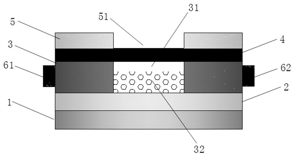
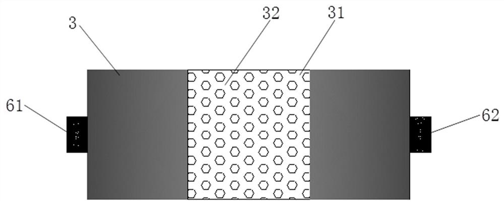
[0036] The photothermal detector of this embodiment is composed of a base layer 1, a dielectric layer 2, a thermally sensitive material layer 3, and a light blocking layer 5 which are sequentially connected from the bottom to the top. The area of the light blocking layer 5 is not less than the area of the heat-sensitive material layer 3, and the heat-sensitive material layer 3 is made of heat-sensitive material, such as image 3 As shown, the heat sensitive material layer 3 is provided with first nanoholes 31, the first nanoholes 31 are filled with precious metal particles 32, the light blocking layer 5 is made of silicon material, and the light blocking layer 5 is provided with A second nanohole 51 with the same nanohole 31, the first nanohole 31 and the second nanohole 51 are positioned opposite each other up and down, and a first electrode 61 and a second electrode 62 are respectively provided on both sides of the heat sensitive material layer 3 for connecting to the outsi...
Embodiment 2
[0045] Based on the photothermal detector structure disclosed in Embodiment 1, this embodiment also discloses a photothermal detector structure, such as figure 1 with image 3 As shown, on the basis of Example 1, a graphene film layer 4 is also connected between the heat sensitive material layer 3 and the light blocking layer 5, and the distance between the graphene film layer 4 and the upper surface of the noble metal particles 32 is not greater than 100 nm .
[0046] Specifically: the graphene film layer 4 is a two-layer graphene. The graphene film layer 4 of the photothermal detector in this embodiment uses a double-layer graphene film. Graphene is a good saturator and absorber, and the double-layer graphite A resonant cavity can be formed between the olefin films, which makes the light travel longer in the cavity. The single-photon absorption coefficient of the double-layer graphene (about 2.1×10 8 m -1 ) Larger than a single layer graphene (about 6.8×10 7 m -1 ) Absorption co...
Embodiment 3
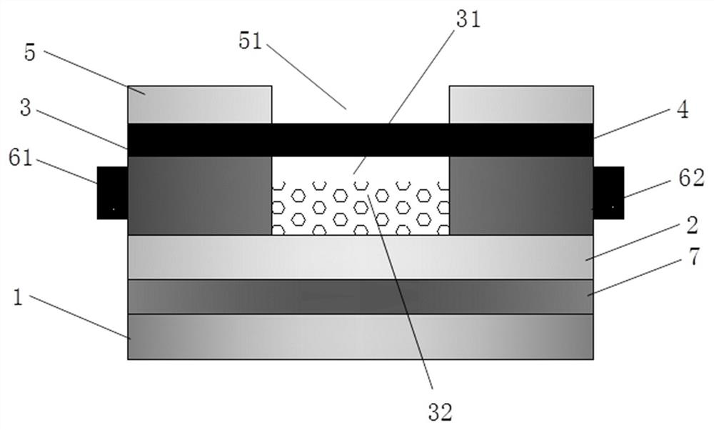
[0050] A photothermal detector structure disclosed based on embodiment 2, such as figure 2 As shown, this embodiment also discloses a photothermal detector structure. On the basis of Embodiment 2, a gold film 7 is also provided between the base layer 1 and the dielectric layer 2.
[0051] Specifically: the photothermal detector of this embodiment is also provided with a gold film 7 on the lower surface of the base layer 1. The coupling between the gold film 7 and the incident light is used to enhance the absorption of the incident light from the upper and lower levels, so that The light absorption effect of the detector in the embodiment of the application is better.
[0052] Such as Figure 4 As shown in (c), the light absorption spectrum of the photothermal detector of this embodiment after the gold film 7 is added, the absorption of each wavelength band has increased, and in embodiment 2, the absorption rate of the absorption mode of λ=820nm is changed from 66% is increased to...
PUM
| Property | Measurement | Unit |
|---|---|---|
| diameter | aaaaa | aaaaa |
Abstract
Description
Claims
Application Information


