

High color rendering white light source structure and manufacturing method thereof
A white light source and high color rendering technology, which is applied in electrical components, circuits, semiconductor devices, etc., can solve the problems of low efficiency of ultraviolet light chips and RGB phosphors, difficulty in meeting low color temperature lighting requirements, and complex drive circuits for chip performance. , to improve the working stability and service life, save part of the packaging process, and achieve the effect of small warping deformation
- Summary
- Abstract
- Description
- Claims
- Application Information
AI Technical Summary
Problems solved by technology
Method used
Image

Examples
Embodiment 1
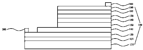
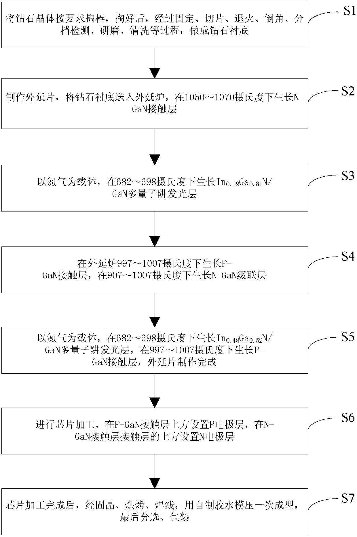
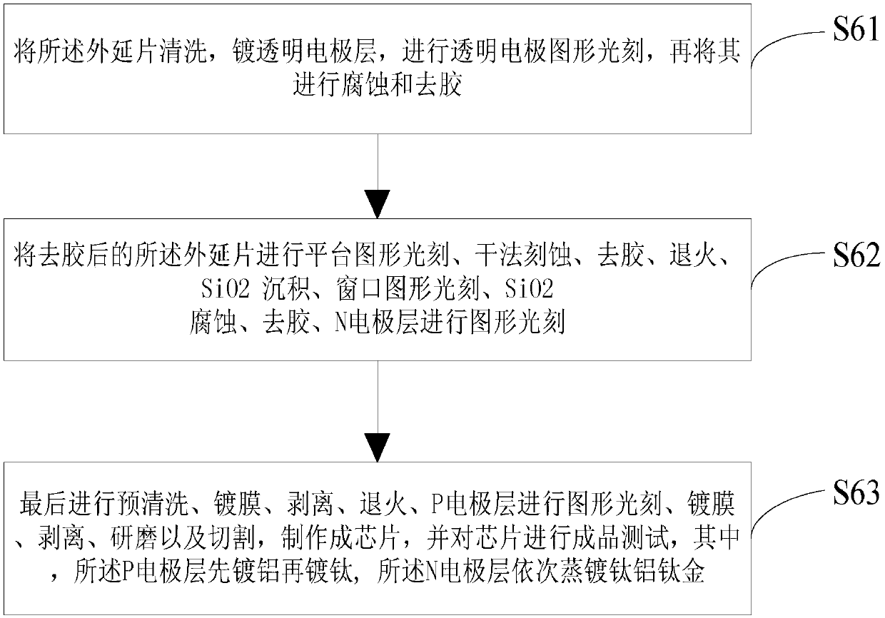
[0082]Digging the diamond crystal into rods according to requirements, and making qualified 2-inch or 4-inch diamond rods through the processes of fixing, slicing, annealing, chamfering, binning inspection, grinding, cleaning, etc. The thickness of the diamond substrate is 150um.
[0083] Put the diamond substrate into the K465i MOCVD epitaxial furnace in a tray, grow the GaBi transition layer at 610 degrees Celsius, and grow the N-GaN contact layer at 1050 degrees Celsius; then use nitrogen as the carrier to grow In at 680 degrees Celsius. 0.19 Ga 0.81 N / GaN (doped zinc, cadmium, silicon, selenium) multiple quantum well light-emitting layer, then grow P-GaN contact layer at 990 degrees Celsius, grow N-GaN cascade layer at 950 degrees Celsius, grow N at 1050 degrees Celsius -GaN contact layer, In grown at 680°C 0.48 Ga 0.52 N / GaN (doped zinc, cadmium, silicon, selenium) multi-quantum well light-emitting layer, growing P-GaN contact layer at 990 degrees Celsius, and the epit...
PUM
| Property | Measurement | Unit |
|---|---|---|
| Thickness | aaaaa | aaaaa |
| Thickness | aaaaa | aaaaa |
| Thickness | aaaaa | aaaaa |
Abstract
Description
Claims
Application Information