Solar cell and preparation method and photovoltaic module thereof

A technology of solar cells and conditions, applied in the field of solar photovoltaic, can solve the problems of insufficient improvement effect and the like

Active Publication Date: 2018-12-14
CSG PVTECH +1
View PDF5 Cites 4 Cited by
  • Summary
  • Abstract
  • Description
  • Claims
  • Application Information

AI Technical Summary

Problems solved by technology

[0003] At present, in mass production, two layers of SiN are plated on the front surface of crystalline silicon solar cells by PECVD method. X film or three or four layers of SiN X The anti-reflection effect is achieved through the passivation effect of the high-refractive-index silicon nitride at the bottom layer and the matching of the refractive index of each layer of silicon n...

Method used


Image

  • Solar cell and preparation method and photovoltaic module thereof
  • Solar cell and preparation method and photovoltaic module thereof
  • Solar cell and preparation method and photovoltaic module thereof

Examples


preparation example Construction

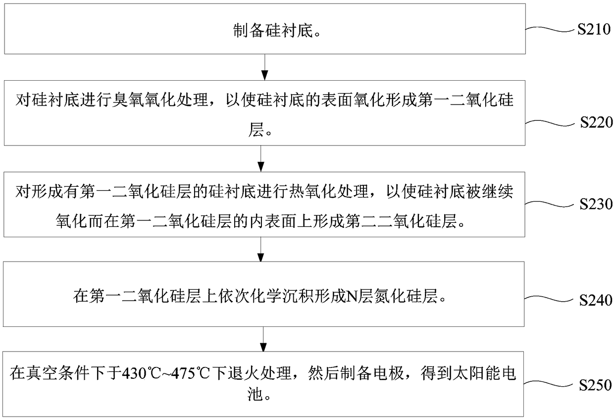
[0043] Such as figure 2 As shown, a method for preparing a solar cell according to an embodiment is a method for preparing the above-mentioned solar cell, and the method for preparing a solar cell includes the following steps:

[0044] Step S210: preparing a silicon substrate.

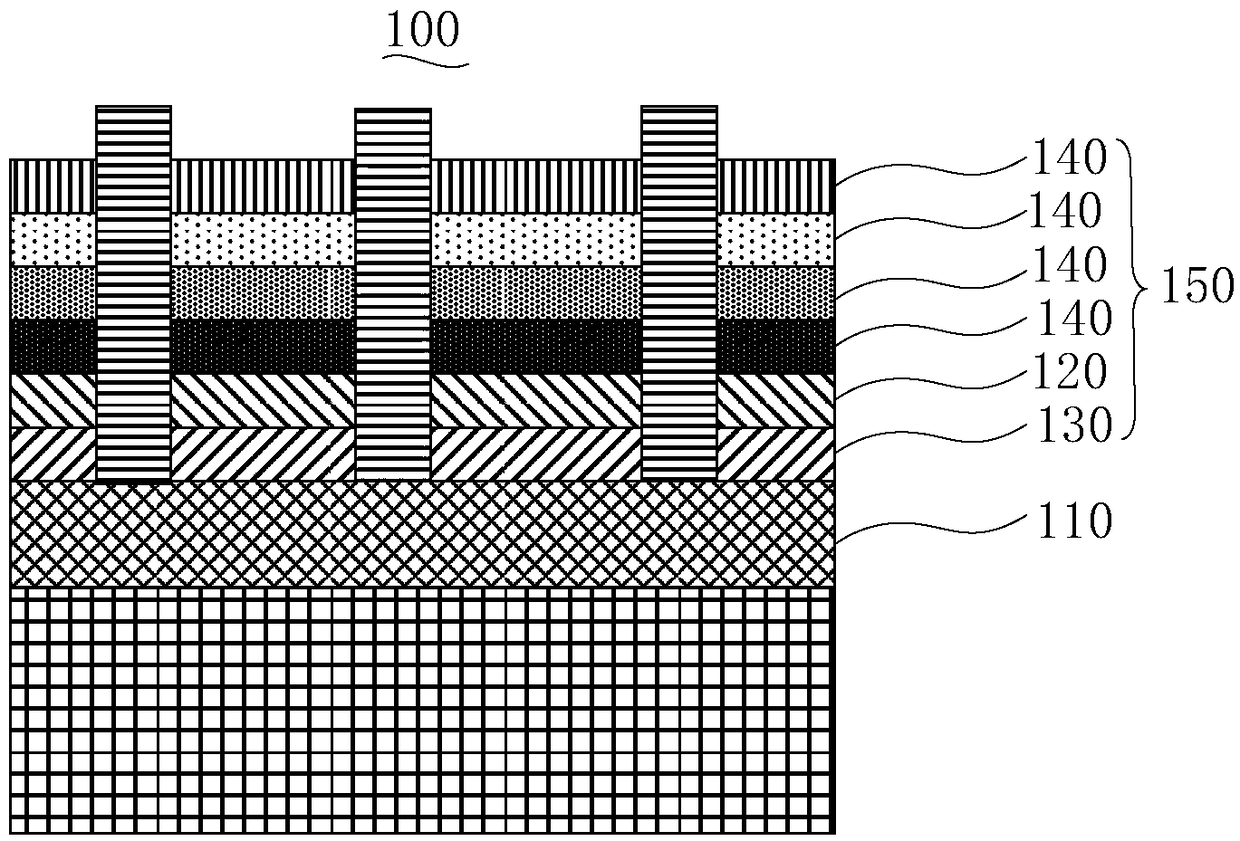
[0045] Specifically, the step of preparing the silicon substrate includes: cleaning the silicon wafer, and texturizing one surface of the silicon wafer to form a textured surface, then performing a diffusion treatment on the textured silicon wafer to form a PN junction, and then treating the silicon wafer Perform edge etching and remove the phosphosilicate glass layer, and obtain a silicon substrate after cleaning. That is, the silicon substrate is a silicon wafer formed with a PN junction. Wherein, the silicon wafer is monocrystalline silicon, polycrystalline silicon or quasi-crystalline silicon. Specifically, the silicon substrate is a P-type silicon wafer.

[0046] Step S220: performing ozone o...

Embodiment 1

[0082] The preparation process of the solar cell of the present embodiment is as follows:

[0083] (1) The original P-type polysilicon wafers cut by diamond wires are cleaned once with conventional hydrofluoric acid and nitric acid adding texturing additives to form a textured surface, and then the textured silicon wafers are subjected to diffusion treatment to form a PN junction. After edge etching and removal of phosphosilicate glass, it is cleaned to obtain a silicon substrate.

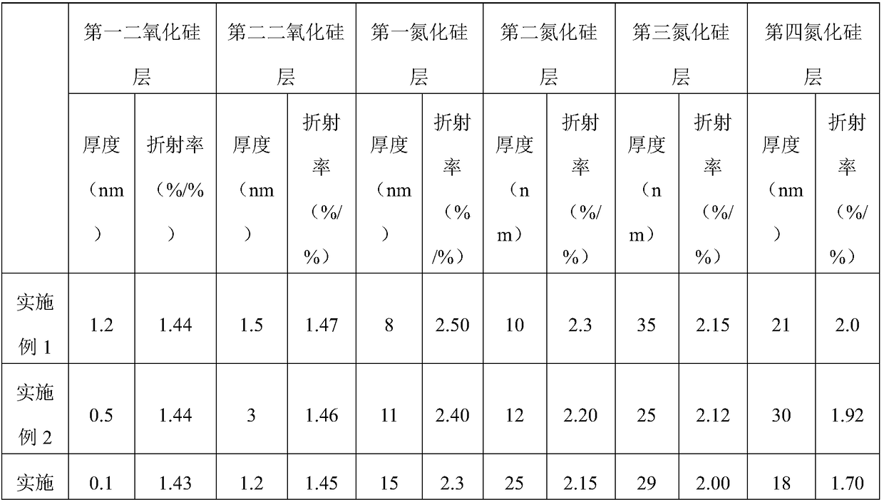
[0084] (2) Utilize an ozone generator to spray the silicon substrate through the spray plate to carry out ozone oxidation treatment, the ozone concentration is 0.3ppm, the distance of spraying is 2 millimeters, and the temperature is 25 ° C, so that the surface of the silicon substrate Can be oxidized to form a first silicon dioxide layer with a refractive index of 1.44 and a thickness of 1.2 nanometers. Wherein, it is the oxygen of 16slm that feeds flow in the ozone generator, and the nitrogen th...

Embodiment 2

[0096] The preparation process of the solar cell of the present embodiment is as follows:

[0097] (1) The original P-type polysilicon wafer cut by diamond wire is cleaned with conventional hydrofluoric acid and nitric acid to add texturing additives to form a textured surface, and then the textured silicon wafer is diffused to form a PN junction. After edge etching and removal of phosphosilicate glass, it is cleaned to obtain a silicon substrate.

[0098] (2) Utilize an ozone generator to spray the silicon substrate through a spray plate to carry out ozone oxidation treatment, the ozone concentration is 0.1ppm, the distance of spraying is 1 mm, and the temperature is 20°C, so that the surface of the silicon substrate Can be oxidized to form a first silicon dioxide layer with a refractive index of 1.44 and a thickness of 0.5 nm. Wherein, the oxygen gas with a flow rate of 1 slm and the nitrogen gas with a flow rate of 10 slm are used as protective gas through the ozone genera...


PUM

PropertyMeasurementUnit
Thicknessaaaaaaaaaa
Thicknessaaaaaaaaaa
Thicknessaaaaaaaaaa

Abstract

The invention relates to a solar cell, a preparation method thereof and a photovoltaic module. A second silicon dioxide layer of the solar cell, a first silicon dioxide layer and an N-layer silicon nitride layer are sequentially laminated on a silicon base layer, and the refractive index of the second silicon dioxide layer is larger than the refractive index of the first silicon dioxide layer. From the first silicon dioxide layer to the first silicon dioxide layer, the refractive index of the N-layer silicon nitride layer decreases in turn, and the thickness of the silicon nitride layer closest to the first silicon dioxide layer is the smallest among the N-layer silicon nitride layers. The conversion efficiency of the solar cell is high and the anti-PID performance is good.

Description

technical field [0001] The invention relates to the field of solar photovoltaics, in particular to a solar cell, a preparation method thereof, and a photovoltaic module. Background technique [0002] Solar power generation is a clean, green and renewable energy source. Under the background of the depletion of traditional energy sources and increasing environmental pollution, solar power generation is becoming more and more popular. However, the most urgent problem facing solar photovoltaic technology is how to reduce costs and increase efficiency faster to achieve the goal of competing with conventional energy sources. In the process of preparing crystalline silicon solar cells, coating a passivation film and a reflective film on the surface of a silicon substrate can effectively reduce surface recombination and light reflection, and improve cell conversion efficiency. [0003] At present, in mass production, two layers of SiN are plated on the front surface of crystalline ...

Claims


Application Information

Patent Timeline
IPC IPC(8): H01L31/0216H01L31/18B82Y20/00B82Y30/00
CPCB82Y20/00B82Y30/00H01L31/02167H01L31/02168H01L31/1868Y02E10/50Y02P70/50
Inventor 赖海文吴娟宋海峰李家兰梁杭伟叶雄新孙小菩
Owner CSG PVTECH
Why Eureka
Try Eureka