An epitaxial growth method for improving the luminous efficiency of a GaN-based LED chip

A technology for LED chips and luminous efficiency, applied in gaseous chemical plating, coatings, electrical components, etc., can solve the problems of low hole concentration, low hole mobility and loss in the light-emitting layer, and achieve improved ionization concentration, The effect of increasing the hole concentration

Active Publication Date: 2018-12-14
XIANGNENG HUALEI OPTOELECTRONICS
View PDF6 Cites 6 Cited by
  • Summary
  • Abstract
  • Description
  • Claims
  • Application Information

AI Technical Summary

Problems solved by technology

At present, the scale of LED production at home and abroad is gradually expanding, and the demand for LED brightness and light efficiency in the market is increasing day by day, but LED still has the problem of low luminous efficiency, which affects the energy-saving effect of LED.
[0003] At present, the traditional LEDs on the market are limited by the

Method used


Image

  • An epitaxial growth method for improving the luminous efficiency of a GaN-based LED chip
  • An epitaxial growth method for improving the luminous efficiency of a GaN-based LED chip
  • An epitaxial growth method for improving the luminous efficiency of a GaN-based LED chip

Examples


Embodiment 1

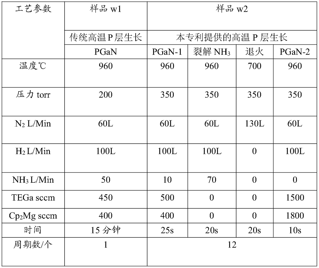
[0048] The invention uses MOCVD to grow high-brightness GaN-based LED epitaxial wafers. Using high-purity H 2 or high purity N 2 or high purity H 2 and high purity N 2 The mixed gas as the carrier gas, high-purity NH 3 As the N source, the metal-organic source trimethylgallium (TMGa), triethylgallium (TEGa) is used as the gallium source, trimethylindium (TMIn) is used as the indium source, and the n-type dopant is silane (SiH 4 ), trimethylaluminum (TMAl) as the aluminum source, and the P-type dopant as magnesium dicene (CP 2 Mg), the substrate is (0001) plane sapphire. The specific growth method is as follows:

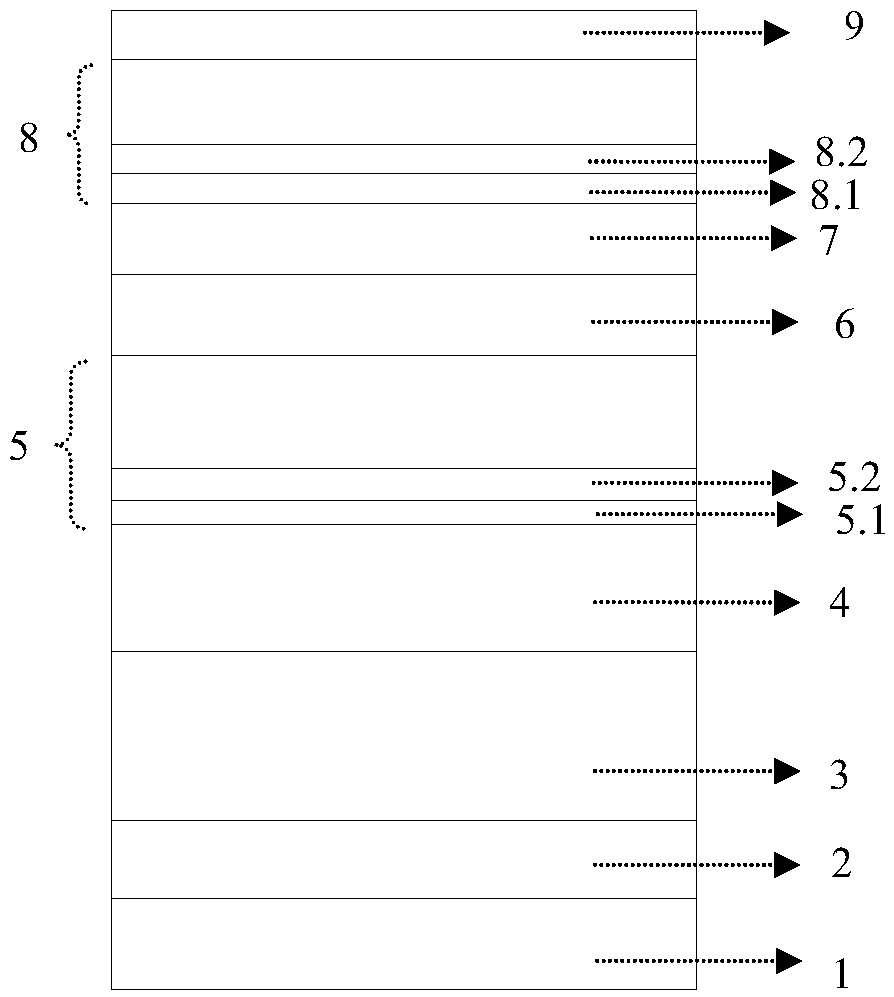
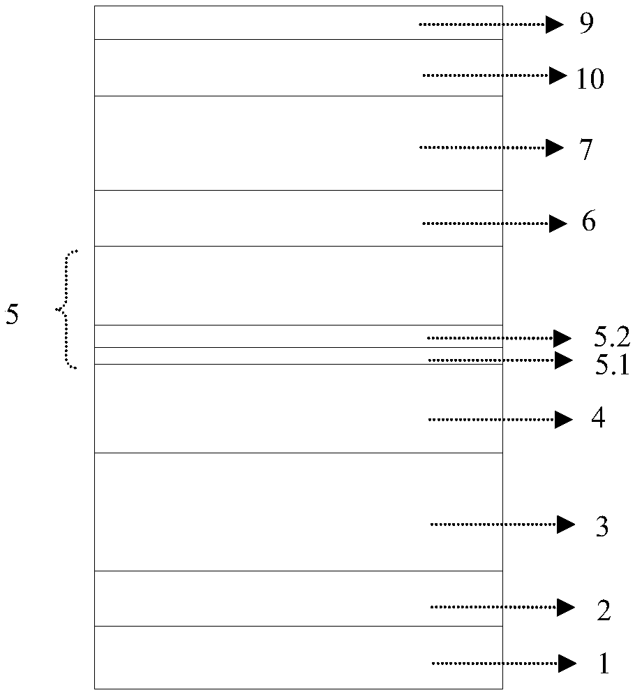
[0049] Please refer to figure 1 with figure 2 , an epitaxial growth method for improving the luminous efficiency of a GaN-based LED chip, comprising:

[0050] Growing undoped GaN layer, growing Si-doped n-type GaN layer, growing low-doped Si n-type GaN layer, growing light-emitting layer, growing low-temperature p-type GaN layer, growing p-type AlGaN layer, ...


PUM


Abstract

The invention discloses an epitaxial growth method for improving the luminous efficiency of a GaN-based LED chip, and includes growing an undoped GaN layer, growing a Si-doped n-type GaN layer, growing a lightly Si-doped n-type GaN layer, growing a luminescent layer, growing a low-temperature p-type GaN layer, growing a p-type AlGaN layer, growing a new p-type GaN layer, growing a high-temperaturep-type GaN contact layer, and cooling, wherein growing the new p-type GaN layer sequentially comprises the steps of growing a high-temperature P-type GaN-1 layer, performing NH3 pyrolysis, performingannealing treatment, and growing a high-temperature P-type GaN-2 layer. Through introduction of the new p-type GaN lay, the n-vacancy of a P structure can be reduced, and Mg-H bonds can be reduced, the ionization rate of Mg of the P structure is increased, the hole concentration of the P structure is increased, and the luminous efficiency of the LED chip is improved.

Description

technical field [0001] The invention relates to the technical field of LED epitaxy design and application, and more particularly relates to an epitaxial growth method for improving the luminous efficiency of a GaN-based LED chip. Background technique [0002] LED (Light Emitting Diode, light-emitting diode) is a kind of solid-state lighting, which is recognized by consumers due to its advantages such as small size, low power consumption, long service life, and environmental protection. The LED epitaxial n-structure provides electrons, and the P-structure provides holes. The electrons and holes are driven by constant current voltage to meet in the light-emitting layer to generate electron-hole pair recombination and release photons. At present, the scale of LED production at home and abroad is gradually expanding, and the market demand for LED brightness and light efficiency is increasing day by day, but LED still has the problem of low luminous efficiency, which affects the ...

Claims


Application Information

Patent Timeline
IPC IPC(8): H01L33/00H01L21/02C23C16/34C23C16/455
CPCC23C16/303C23C16/455H01L21/0242H01L21/0254H01L21/02579H01L21/0262H01L33/007
Inventor 徐平
Owner XIANGNENG HUALEI OPTOELECTRONICS
Why Eureka
Try Eureka