A memristor switch device based on a-TSC: O ceramic film and a preparation method thereof

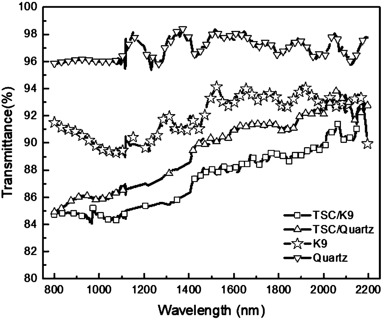
A technology of ceramic thin films and switching devices, applied in electrical components and other directions, can solve problems such as research reports on applications in the field of optoelectronics that have not been seen, achieve good near-infrared transmittance, achieve large-scale production, and broaden the selection range.

Active Publication Date: 2018-12-21
UNIV OF ELECTRONICS SCI & TECH OF CHINA
View PDF6 Cites 2 Cited by
  • Summary
  • Abstract
  • Description
  • Claims
  • Application Information

AI Technical Summary

Problems solved by technology

Based on the above content, we can see that the existing Ti 3 SiC 2 The development and research of applications mainly focus on high-temperature structural materials, electrode materials, machinable ceramic materials, anti-friction component materials and anti-corrosion protective layers, and there are no research reports on their application in the field of optoelectronics

Method used


Image

  • A memristor switch device based on a-TSC: O ceramic film and a preparation method thereof
  • A memristor switch device based on a-TSC: O ceramic film and a preparation method thereof

Examples


Embodiment 1

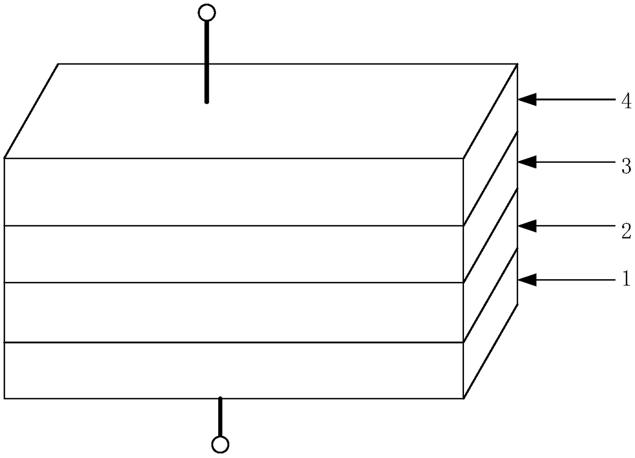
[0031] This embodiment provides a memristive switch device, such as figure 1 As shown, its structure from bottom to top is "ITO slide 1, a-SiOx Thin film 2, a-TSC:O thin film 3, a-TSC thin film 4 "vertical four-layer structure," a-SiO x Thin film 2 / a-TSC:O thin film 3" double-layer structure acts as a double resistance layer (that is, the dielectric layer of the memristive switching device).

[0032] This embodiment provides a method for preparing the above-mentioned memristive switch device, and the preparation process includes the following steps:

[0033] Step A: prepare the ITO glass slide 1 as a transparent substrate with a bottom electrode, and perform cleaning and drying according to a standard process;

[0034] Step B: using a silicon target as a raw material target, oxygen and argon as a working gas, and depositing an a-SiOx film 2 on an ITO glass substrate 1 by reactive radio frequency sputtering as a first resistive layer;

[0035] Step C: Using Ti 3 SiC 2 Polyc...

Embodiment 2

[0052] This embodiment provides a method for preparing a memristive switch device, and the preparation process includes the following steps:

[0053] Step A: Prepare a K9 glass substrate as a transparent substrate, and perform cleaning and drying according to standard processes; then deposit an ITO film on it as a bottom electrode;

[0054] Step B: using a crystalline silicon target as a raw material target, oxygen and argon as a working gas, and depositing an a-SiOx film on the ITO film by reactive radio frequency sputtering as the first resistive layer;

[0055] Step C: Using Ti 3 SiC 2 The polycrystalline powder is used as the raw material target, oxygen and argon are used as the working gas, and the a-TSC:O film is deposited on the a-SiOx film by reactive radio frequency sputtering as the second resistive layer. The specific operation is as follows:

[0056] C1: Target preparation:

[0057] Ti 3 SiC 2 Add the powder into deionized water and stir evenly to obtain Ti 3...


PUM

PropertyMeasurementUnit
thicknessaaaaaaaaaa
thicknessaaaaaaaaaa
thicknessaaaaaaaaaa

Abstract

A memristor switching device based on a-TSC: O ceramic film and a preparation method thereof belong to the technical field of photoelectric devices. On the basis of the traditional memristor switchingdevice structure, the invention innovatively proposes a dielectric layer structure of a TSC: O thin film/a SiOx thin film, which widens the selection range of the dielectric layer material of the memristor switching device. As the resistivity of the a-TSC: O film is adjustable in a wide range, and the a-SiOx thin films are transparent and can provide oxygen vacancy electromigration channels, thea-TSC: O films have good resistance and can be used as the dielectric layer of memristor switches. At the same time, due to intrinsic a-TSC ceramic thin film has excellent conductivity and near infrared transmittance, it can be used as top electrode material to construct near infrared transparent memristor switching device together with top electrode formed by transparent conductive thin film. Inaddition, the memristor switching device provided by the invention has the advantages of simple preparation process, low cost and high reliability, and is favorable for realizing large-scale production.

Description

technical field [0001] The invention belongs to the technical field of optoelectronic devices, and in particular relates to a memristive switching device based on a-TSC:O ceramic film and a preparation method thereof. Background technique [0002] As a new type of nonlinear device, memristor has received extensive attention from researchers. So far, materials such as Ag, Cu, Au, Pt and W have been used as their electrode materials; a-Si, a-SiO x and TiO 2 Isodielectric films are common resistive layer materials for memristive switching devices. In recent years, researchers at home and abroad have constructed and prepared a variety of memristive switching devices with excellent resistive switching functions based on various electrodes and resistive layer materials, making them the darling of next-generation memory technology. [0003] Ti 3 SiC 2 It is a ternary layered carbide, which is the only MAX phase material containing Si element, and has both ceramic and metal pro...

Claims


Application Information

Patent Timeline
Patent Type & Authority Applications(China)
IPC IPC(8): H01L45/00
CPCH10N70/841H10N70/881H10N70/011H10N70/026
Inventor 次会聚陈奕丞宋宇浩刘诚李东阳李伟
Owner UNIV OF ELECTRONICS SCI & TECH OF CHINA
Why Eureka
Try Eureka