A semiconductor memory aging test system and method

An aging test and memory technology, applied in static memory, instruments, etc., can solve problems such as no test process recording and management analysis, no test process and result management analysis, no mention of high and low temperature aging test solutions, etc. Test signal quality, improve scalability, reduce temperature shock effects

Inactive Publication Date: 2018-12-25
武汉精鸿电子技术有限公司
View PDF15 Cites 24 Cited by
  • Summary
  • Abstract
  • Description
  • Claims
  • Application Information

AI Technical Summary

Problems solved by technology

[0010] The Chinese patent with the publication number CN102467973A discloses a memory testing method and device, which mentions that when the memory is aging, the heat generated by its own power consumption is used to control the aging temperature, so as to solve the problem of uneven temperature distribution and temperature error caused by external heating. It is mentioned that the controller and signal generator are used to test the memory, and the row-column matrix control method is mainly used; however, it does not involve the recording and management analysis of the test process, and this method is not suitable for low-temperature aging tests and has certain limitations
[0011] The Chinese patent with the publication number CN107271879A discloses a semiconductor chip aging test device and method, which is a method for reducing the transmission distortion of the test clock signal, mainly by moving the high-frequency crystal oscillator that generates the clock signal to the vicinity of the chip socket under test. And multiple clock sources can be selected through the multiplexer, so that the chip can be tested for durability aging at room temperature; there is no mention of high and low temperature aging test solutions, and there is no management analysis of the test process and results

Method used


Image

  • A semiconductor memory aging test system and method
  • A semiconductor memory aging test system and method
  • A semiconductor memory aging test system and method

Examples


Embodiment Construction

[0053] In order to make the object, technical solution and advantages of the present invention clearer, the present invention will be further described in detail below in conjunction with the accompanying drawings and embodiments. It should be understood that the specific embodiments described here are only used to explain the present invention, not to limit the present invention. In addition, the technical features involved in the various embodiments of the present invention described below can be combined with each other as long as they do not constitute a conflict with each other.

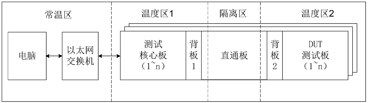
[0054] refer to Figure 1 to Figure 5 , to describe an embodiment of the semiconductor memory burn-in test system provided by the present invention.

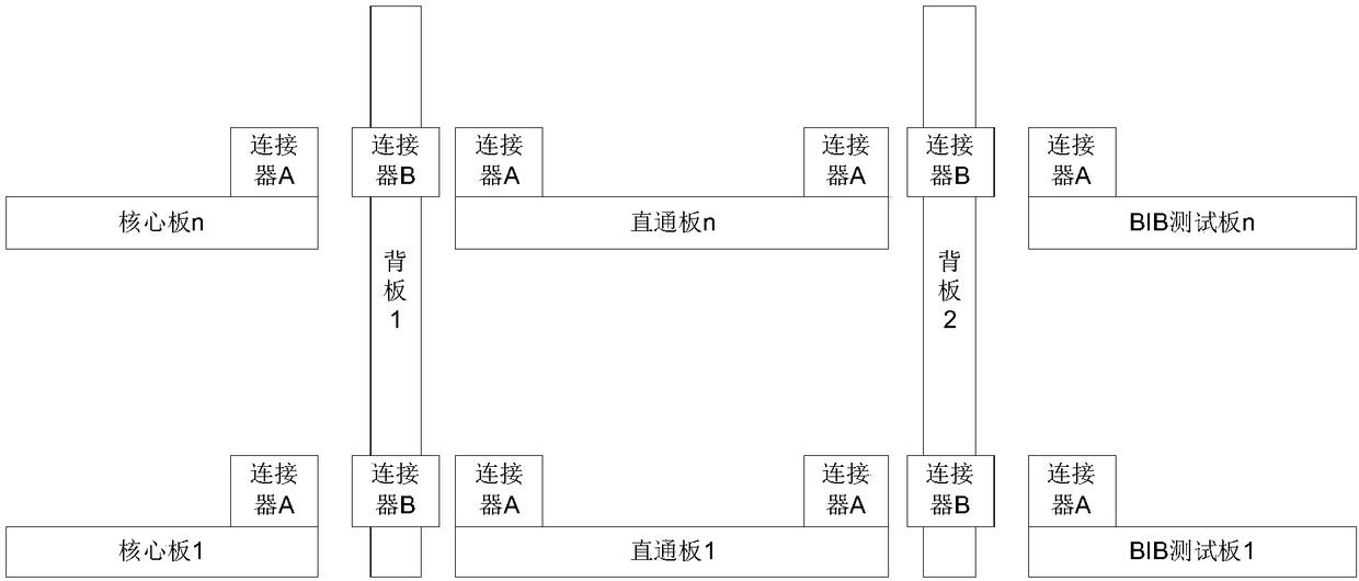
[0055] The semiconductor memory burn-in test system provided by the embodiment includes a host computer, a switch, a test core board, a first backplane, a test board, and a second backplane;

[0056] The host computer is used to run the test sof...


PUM


Abstract

The invention belongs to the technical field of semiconductor memory test and discloses a semiconductor memory aging test system and a method. The system comprises a test core board and a test board.The test core board generates a t signal and a power signal according to that instruction of the upper computer, and after the test signal and the power signal are adjusted, the test signal is provided to a DUT, and the DUT output signal is compared with a preset value to obtain a preliminary test result which is partitioned and stored, and is uploaded to the upper computer; the test board is usedfor carrying DUT, providing clock signal and chip selection signal for DUT. A single test board is provided with a plurality of t bits, and DUT aging test can be carried out by a single DUT or by multiple DUTs at the same time. By outputting various types of test signals on the test core board, and adjusting the delay time of the test signal, strengthening the processing of driving, waveform control, and compensating the power signal, and storing the test results in the partitioned storage area respectively, the functions of management of single DUT test process control and failure analysis in aging test are realized, and the same test number of DUT is increased, which reduces the test resource overhead.

Description

technical field [0001] The invention belongs to the technical field of semiconductor memory burn-in test, and more particularly relates to a semiconductor memory burn-in test system and method. Background technique [0002] Semiconductor memory has a certain failure probability, and the relationship between the failure probability and the number of times of use conforms to the characteristics of the bathtub curve. The failure probability of the memory is high at the beginning of use, and the failure probability is greatly reduced after a certain number of times of use, until it is close to or reaches its use. After the lifetime, the failure probability of the memory will increase again. So far, no memory manufacturer has dared to ignore the failure problem of semiconductor memory. Generally, the aging test (Test During burn-in, TDBI) is used to accelerate the occurrence of memory failure probability, and directly let it enter the product stable period to solve this problem. ...

Claims


Application Information

Patent Timeline
Patent Type & Authority Applications(China)
IPC IPC(8): G11C29/56
CPCG11C29/56
Inventor 陈凯张庆勋邓标华周璇
Owner 武汉精鸿电子技术有限公司
Why Eureka
Try Eureka